I then mod’d txshield demo to sample A5 instead of A4 so I could then directly compare the unfiltered (A1) with the filtered (A5). It made things quite a bit worse which is not surprising given all those dangly legs… it violates all the rules of keeping the filter near the input pin (or carefully laying out the traces between the filter and the input pin). If you had some SMDs and better soldering skills, you could potentially glue one right alongside A5 on the shield and see if it improves things (although that’s still a ways away from the CPU pin).
But it revealed a few things… the reported noise on Irms was worse than the signal suggested it should be, and that led me to find those bugs fixed above. Also that filter drags down A1 slightly (it started reading lower than A2 and A3 with all wrapped around the calibrator loop)… specifically the 100nF cap to GND.
So when designing your input conditioning circuitry I think you do need to be aware of the filter characteristics… it affects total source impedance.
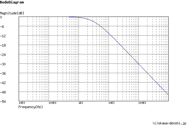
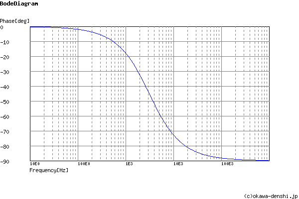
I have just played with an online component calculator for LPF’s and apparently the 1K and 100nf combo would give you a “cut-off” frequency (where signal is 3db down) of just over 1,592Hz.
Since the resistor (I assume) would add to the impedance I’m guessed the cap was lowering the impedance, checking a capacitor impedance online calculator, it seems the 100nF cap has an impedance of just under 31831R at 50Hz. Is that what’s doing it?
Playing with a few values I’m guessing that a lower cap value is desirable? Sticking with the 1K resistor that we already have in the design for input protection, and a cut-off of 7KHz (midway between the 4-10KHz mentioned above) we would want something like a 22.75nF cap which has an impedance of nearly 140K, so it shouldn’t impact the overall impedance? Or will it? (I have very little memory of the small amount of electronic theory I did many years ago).
Obvious questions that arise from that is, would the resister still work to protect the input? should the protection diodes be before or after the filter? seems everything needs to be “as close as possible to the input pin”.
I’m just doing these calc’s to get my own head around what’s needed, I would hope someone with a better understanding will calculate the actual values needed.
The 4-10KHz mentioned earlier, does that relate to the 50/60Hz directly or to the sampling frequency? I thought that a anti-alias filter was tied to the sampling frequency, or does the anti-alias filter become redundant with a lower frequency LPF?
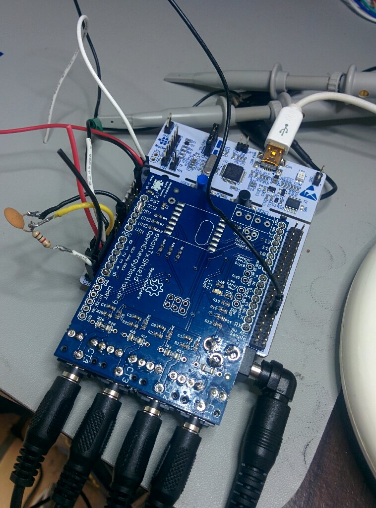
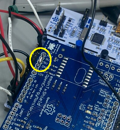
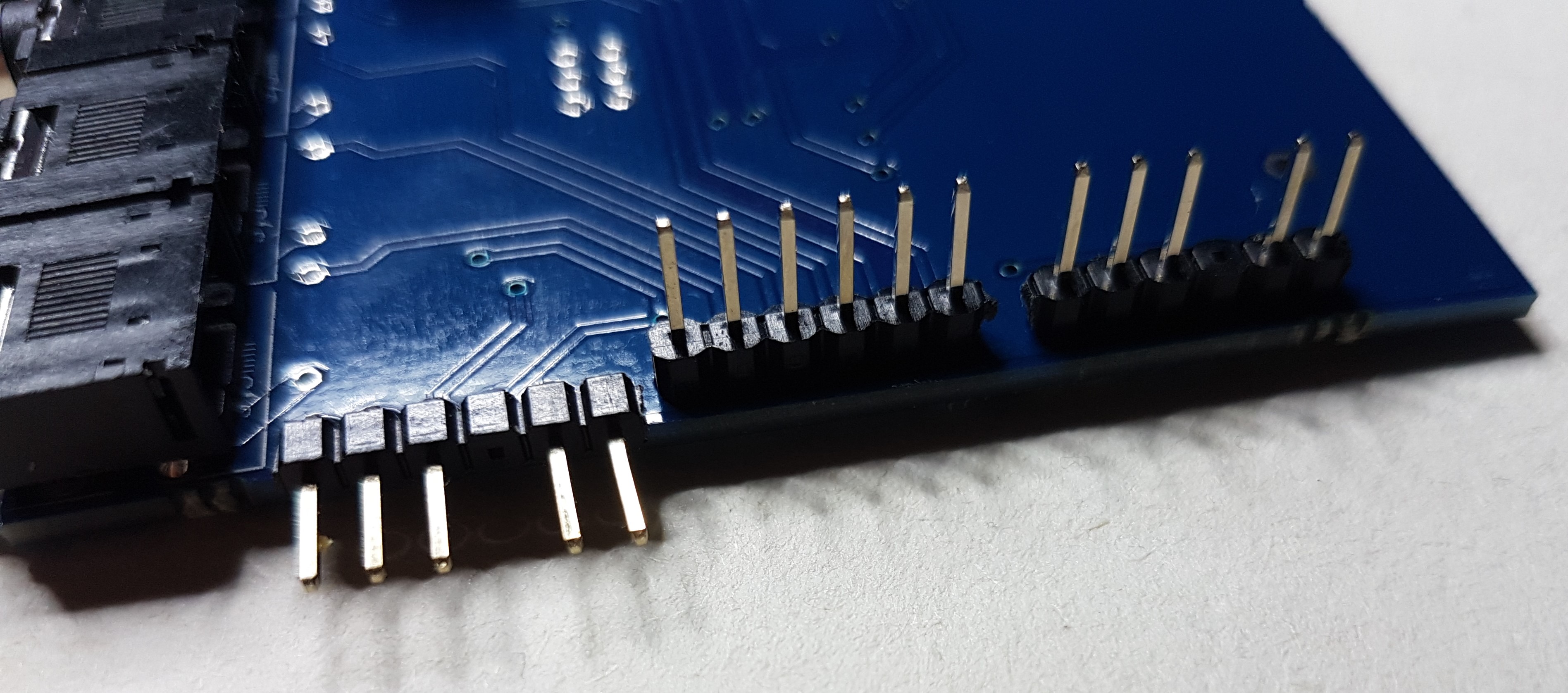
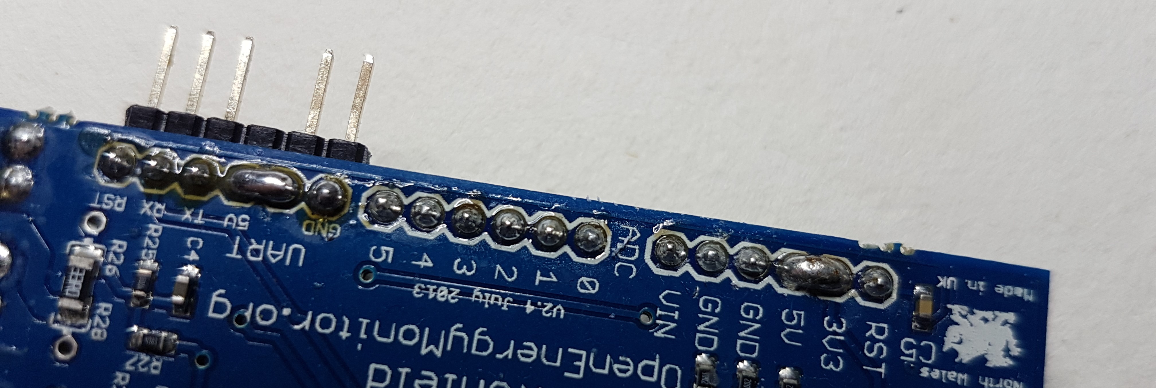
That is a solder bridge to link the 5v and 3.3v rails of the shield because it was originally 5v powered, now all 3.3v. under that solder bubble, the 5v header pin has also been removed so that both the 3.3v and 5v rails of the shield get their power from the 3.3v rail of the STM32.
[edit - When I fitted a 6pin FTDI header I did the same, @Trystan did the original mods.]
Thanks for the skinny on that, PB.
Not having followed the development of the “shield” I wasn’t aware of the mods.
Time to get out the soldering iron and wire cutters.
The anti-alias filter is related to both. It should not attenuate any signal of interest, yet it should completely remove all frequencies above the sampling frequency. An ‘alias’ is a generated when a signal above the sampling frequency is sampled, it is “folded” back at the sampling frequency and appears in the output as a lower frequency. So say the sample rate is 100 k samples/second, a signal at 140 kHz will appear as a signal at 60 kHz. I think the recommendation is the attenuation at sampling frequency should be 40 dB (× 0.01) if a first order (plain RC) filter is used, so the corner frequency at which the loss is 3 dB (× 0.707) is 2 decades below the sampling frequency. My feeling is we should not be too interested in harmonics of mains above the 25th (1250 or 1500 Hz). If we accept a 10% error at that, it’s 1 dB (near enough), and that implies a corner frequency of 3 kHz or higher.
dBC has been using the terms interchangeably. An anti-alias filter is low pass, a low pass filter will function as an anti-alias filter if it attenuates frequencies above the sampling frequency sufficiently.
The filter is nothing more than a variable attenuator with one element whose value depends on frequency. At d.c., the low pass filter is just a series resistor, at very high frequencies, it looks like a series resistor followed by a dead short to ground. The impedance presented to the ADC therefore starts out as the resistor in series with the source, and falls with frequency (but in a non-linear way).
Yes, and don’t for a minute take that as a recommendation it was merely what I could find in a hurry, and I wanted to err on the side of over-filtering (i.e. lower corner frequency) than under-filtering in order to see if I could observe any difference. Robert’s suggested bandwidth limits seem reasonable to me.
Yes, pretty much. Just to clarify, I was using A1 (CT1) as my source signal, and feeding a filtered version of that to A5. The 1K series resistor is downstream of A1. But the 100nF cap connects directly from A1 to GND. It’s that cap that drags down the A1 reading.
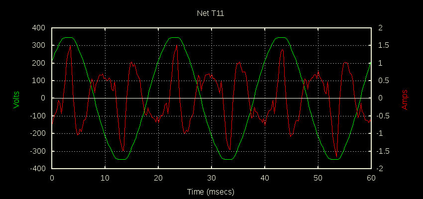
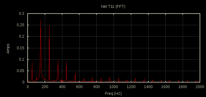
Going back to the original standard txshield demo with 4 CTs wrapped around a 10A signal it looks like this:
As you say, presumably you’d see the same sag in channel 0 if you replaced the cap with a 31K R. I think I’m basically putting too big a load on the CT circuitry output.
I don’t think the protection diodes need to be particularly near the pin. In fact, having some resistance between them and the input pin may make them more effective. AFAIK nobody here has researched the requirements there, but it’ll almost certainly be different from what was required on the AVR. We’d need to find the injected current limits, and at what voltage the internal protection diodes start to conduct.
I concur with Robert’s comments on sampling frequencies. There may be situations where you sample faster than you want/need to, not in order to pick up higher harmonics, but get higher resolution on the V signal to assist with interpolation, or because it’s just the way the dividers/ADC-slot maths worked out. For example the current txshield demo steps through this 2-slot sequence:
at 29.316kHz. So V1 is being sampled at 29kHz, while each of the CTs are being sampled at half that rate, 14.66kHz. They’re all faster than needed to meet Robert’s suggested bandwidth, but would slow down if we add more slots to handle more channels, and more V phases. If we added so many more slots (max 16) that the sampling rate became too slow, then we could just bump up the ADC clock.
Knowing that the sampling rate per channel might be liable to will go down as more channels get added to the scan, my thinking was it’s better to set the anti-alias filter based on the minimum acceptable performance of the wanted signal than to set it on the anti-alias criteria. If it looks as if it might fail that - and it does, based on a less than 30 kHz sample rate, then we should be looking at a higher-order filter.
@dBC, are you able to do a Fourier analysis of that awful spiky current waveform you refer to occasionally and report the levels of the various harmonics? That should give a guide to the performance we should be aiming for.
We’ve got some headroom in the ADC clock speed. It can run 2x or 4x faster than we’re currently running it in the txshield demo. So for example, if we were to go from a 2-slot sequence to a uniquely populated 16-slot sequence and change nothing else, the sampling rate would be 1/8th what it currently is (14.66kHz / 8 = 1.8kHz). But we could run the ADC 4x faster than I currently am (72MHz instead of 18MHz), in which case it would be just 1/2 what it currently is (14.66kHz / 2 = 7,33kHz).
The other place we’ve got potentially huge headroom is in S&H charge time. Currently that is set to the maximum: 601.5 cycles. The entire conversion takes 614 cycles, so it’s currently pretty much all charge time. How low we can take that depends on how low we can get the source impedance of the signal, but currently at least, it’s set as conservatively as it can go.
There are two that spring to mind. The first is a CT wrapped around the main feed from the street when there is close to perfect balance between PV output and consumption. In that case the inverter is providing pretty much all the fundamental stuff, and the grid is left to supply all the harmonics. That seems to be one case where you can quite legally violate all the rules about how much energy should be in the harmonics Vs the fundamental. That looks like this:
That’s not a logarithmic scale on the FFT, just straight Irms at each harmonic. Also note the sample data is only 4k samples/sec so we can’t see what’s above 2kHz.
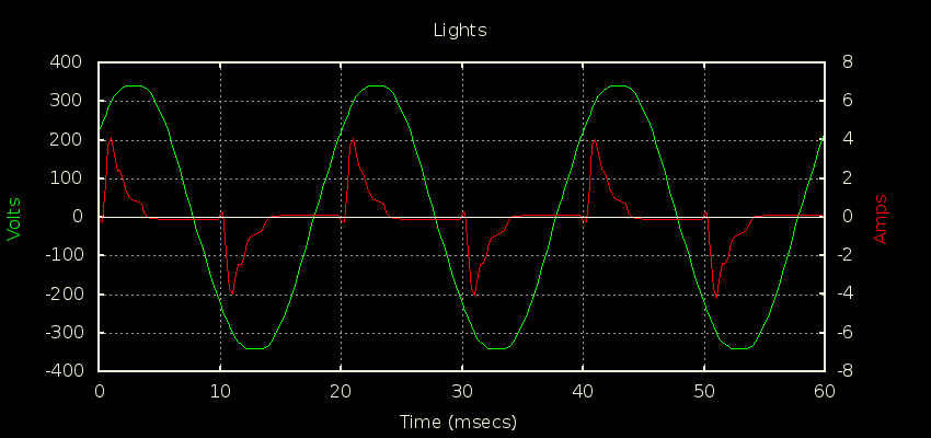
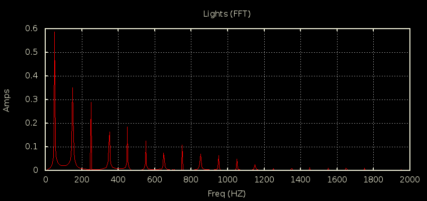
The second one is the lighting circuit when there’s a bunch of CFLs on. It looks like this:
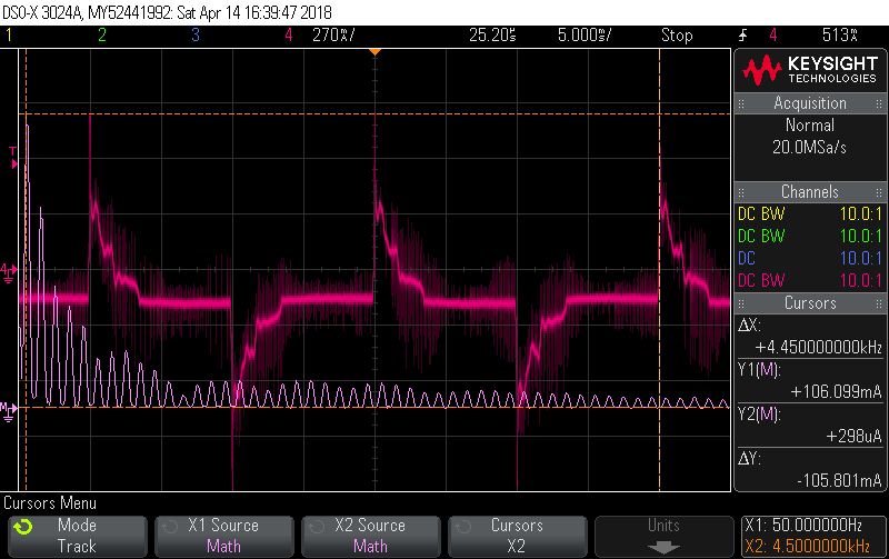
For some sense of scale, the two cursors are at 50Hz (106mA) and 4.5kHz (298uA). You can ignore the Red trace, it’s the signal in the time domain to verify I’m looking at a typical enough specimen (looks close enough to what the energy monitor reports for the lighting circuit when there’s about 200W worth of these things on). The cursors are tracking the FFT (Violet).
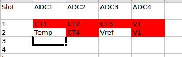
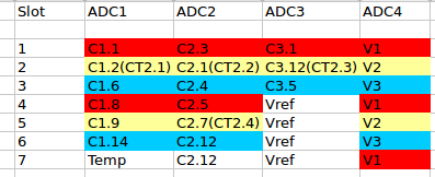
I figured it might be worth loading up the processor with more channels to sample to see what performance was like. So demo10 is a rudimentary 3 phase version, with 15 CT channels, each one hardcoded to a particular phase (5 per phase).
I’m still just using the emonTX shield to drive mine, so only 4 CTs and one V input are being driven, the rest are all floating, but it is at least doing the maths on all 15 channels for timing purposes. I’ve numbered the channels 0 through 14 starting in the top left corner of the slot diagram above, so the relevant channel numbers for the shield CTs are 3, 4, 5 and 12 (the ones with brackets in their names) and they’re all on the Yellow phase (V2). Since the others are undriven, I currently only print out those 4 channels, so the output now looks like:
The ADCs are stepping through each slot at 8.53 usecs, so each CT is being sampled every 59.7 usecs (7 x 8.53 usecs, or 16.75kHz). ADC4 ensures each sample has a corresponding V sample to go with it.
Since this thing has so much RAM I’ve left the DMA buffers at 200 sequences, so 200x7x4x2 = 11,200 bytes. The size of that datastructure also gets displayed at boot time:
emonTxshield Demo 1.10
Patch PA0 through to PB14 for V!!!
DMA buffs: 11200 bytes
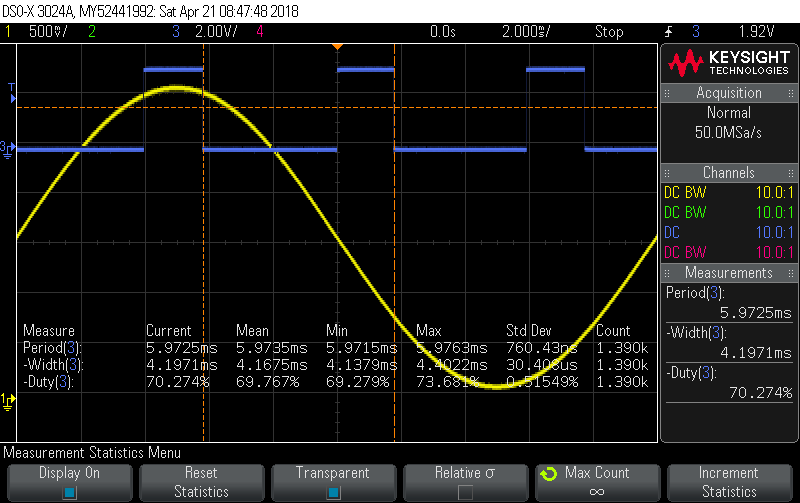
The interrupt still comes in every 100 sequences, so every 5.97 msecs, and it takes about 3.7 4.2 msecs to process the 1500 V,I pairs, so I guess you could say the cpu is about 62% 70% occupied doing the power maths on 15 continuous channels. That doesn’t include any phase shift calculations as it still uses the inadequate one-size-fits-all-channels ADC lag technique for that. And it’s not particularly optimised (other than to do everything in 64-bit integer maths) so an emonlib may well do better, but I figure it’s a basic estimate of the performance available, given it does the all the basics (Vrms, Irms, RealPower etc.). txshield_demo_10.tar.gz (901.0 KB)
It occurred to me that with nothing driving the other two V inputs the power-maths state machine for some of those channels might have been stuck in waiting-for-zx state which is a faster path through the ISR. So I removed the shield, and drove all 3 VT inputs with the signal generator. In the trace below Blue is the LED output and low means it’s in the ISR handler doing the maths, high means it’s in the main loop looking for something to do. You can see the duty cycle is actually very close to 70%, so I’ve corrected the quoted figures in the previous post to reflect that.
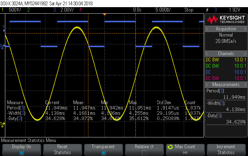
Unsurprisingly, halving the sample rate (from 16,752 samples/sec per CT to 8,376 samples/sec per CT) takes the cpu load from 70% down to 35% for the 3V + 15I case, so there really is still a lot of headroom.
Another way of looking at this would be to mock up the code to dump the results to a serial port for the maximum number of channels which would show what headroom there is from the other perspective. Although I’d expect it to be almost all of what you are already seeing.
You’d probably also want to add in the code to read some DS18B20s and report those results as well.
While I haven’t tried it, I think these stm32 processors are well equipped to deal with OneWire. Dallas have long had a Tutorial 214 on how you can offload all the nasty OneWire usec bit timing into a uart. Each byte passed through the uart represents a single OneWire bit.
The difficulty with that is it requires an open drain output on the uart’s tx signal and most uarts don’t support that natively, so an external buffer is required. The good news is the stm32s uarts support it natively… they have a mode called “Single Wire (Half-Duplex)” which ties the rx and tx together and connects them both to a GPIO pin configured for “Alternate Function Open Drain”.
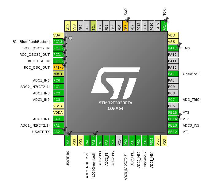
The F303 that @pb66 chose is blessed with lots of uarts, although not all of them seem to be able to use the DMA controllers (or perhaps the DMA controllers are running out of channels running the 4 ADCs). Given that one uart byte represents one OneWIre bit I think you definitely need the DMA controller support.
A quick check in the GUI permits two uarts with full rx/tx DMA support alongside the 4 ADCs. So I think you could actually run two OneWire buses (each with multiple slaves) with very little cpu overhead, well at least not the carefully timed, usec-delays-with-interrupts-off type overhead usually associated with OneWire. Everything else to do with OneWire is not timing critical and can be done in the main loop at your leisure. A possible pinout for that would look like:
With presumably even more options available for the larger pin-out device if that’s what’s been chosen. If I find time, I’ll try to add two OneWire buses to the txshield demo as a proof of concept.
I’m assuming that for a system that is being envisaged one OneWire bus would be adequate, meaning the other uart would be used to dump the results to a serial port to hand them over to say an emonESP to do the networking.
So basically the only thing really taking up any cpu would be dealing with the samples. So as you said earlier plenty of headroom.
Back to the thought I posted some time ago then of a massively distributed bitcoin mining app to pay for the emoncms.org servers.
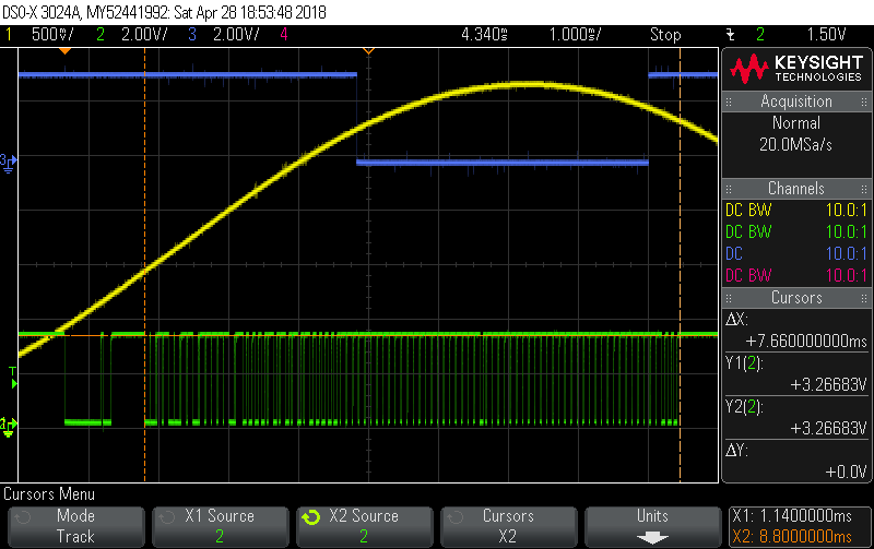
I had a chance to have a play with it, and I’ve got to say it’s an extremely solid way of doing OneWire. The trace below is basically the same as the last one, but with OneWire added, so 3V+15I each being sampled at 8,376 samples/sec. The Yellow and Blue traces are the same as in the picture a couple posts back, with Blue indicating “power maths load”… currently running at about 35% at those sampling rates. Blue low means we’re inside the ADC/DMA ISR grinding our way through 1500 V,I pairs and Blue high means we’re in the main loop looking for other stuff to do.
The new Green trace below is the OneWire bus with a single DS18B20 connected to it. You can see it takes about 7.66 msecs to read the 9 byte scratch pad. Right bang in the middle of that, the ADC/DMA ISR fires and we go off to grind through all the maths (Blue goes low), but it makes no difference to the OneWire transactions which continue on autonomously. Soon after we return from the ADC/DMA ISR, the DS18B20 data is available for processing, with good checksums regardless of CPU load.
Probably true, although for some topologies two buses might be an advantage. At any rate, with the UART-offload techniques there is effectively no overhead to having a second OneWire bus. The overhead is all per-DS18B20 whether they’re all on one bus, or spread across two. So I guess it can be left to the system designer as to how many OneWire buses they want to support.