STM32 Development

This is great to hear!

I see from the repo that you are using a NUCLEO-F401RE development board which has a STM32F401RET6 fitted.

Although the F4 range are faster more powerful MCU’s the board I choose for testing was the NUCLEO-F303RE running slightly slower and with less SRAM because the ADC specs were far more appealing.

The F401 has only one 12-bit ADC with up to a max of 16 channels and a max speed of 2.4msps where as the F303 has 4 12-bit ADC’s with a potential fore up to 40 channels and a max speed of a whopping 18msps. That’s 7.5x as many samples per second from a slower MCU. The 64-pin package on the NUCLEO-F303RE dev board allows access to 22 ADC channels (you need to 128pin package to access all 40)

The F303 also has 4 op amps that can be used as programmable gain amps or perhaps use one for the mid-rail voltage instead of voltage dividers.

Did you have to modify the shield at all as that was designed for an Arduino running at 5v? eg the voltage dividers to the RFM would need bypassing and the burdens changed to suit 3.3v?

Maybe I should consider grabbing a shield for initial dev’ing on the STM? I was actually thinking about doing a short run of 10 or 20 boards to break out 18 adc’s via the ST Morpho connectors with some headers for the mid-rail and voltage dividers so we could try out and compare the onboard op amp options.

These devices have an internal voltage ref calibrated in production and since we have the increased resolution (10bit to 12bit) we might be able to use a smaller input range and use much lower value burdens which could remove much of the phase shift from the CT’s, yes there is a potential for more noise, but I wonder if the result would be better or worse?

1 Like

Some other threads of interest

Best hardware option for multiple CTs & WiFi

STM32 Boards for Energy Monitoring

Success using the STM32F103 microcontroller

2 Likes

Yes, don’t read too much into this. Is just what we had laying about in the lab. I think Ken Boak (NanodeRF designer) gave us a few years ago. We didn’t specifically select it. I see there are lots of different variants.

Yes, @TrystanLea jumpered the 5V rail to 3.3V . We’re not using the RFM. Burden resistor value is not optimal but ok for testing.

A couple of pictures of the prototyping :slight_smile: I was meaning to write up last Friday’s meeting before posting this, as the reason for Glyn and my action on this comes out of your encouragement to do so @pb66, @Robert.Wall @Paul and noting yours and @dBC’s post here . Last time we tried to get the STM32 up and running with Ken Boak’s help we didnt get very far as the toolchain wasn’t quite there yet for Arduino/PlatformIO.
STM32 F401RE and EmonTx Shield:

As well as removing the 5v pin and putting a solder jumper across from 3.3v to 5v I needed to make some minor changes to EmonLib to get it to run the ADC at 12bits rather than 10bits. For some reason analogRead seems to return only 0-1023?, while adc_read_value returns the full 0-4095.
I saw @mel asked a related question here and here.

Provisional EmonLib STM branch: GitHub - openenergymonitor/EmonLib at STM32
Diff comparison: https://github.com/openenergymonitor/EmonLib/compare/STM32

Basic example:

// EmonLibrary examples openenergymonitor.org, Licence GNU GPL V3
#include "EmonLib.h"             // Include Emon Library
EnergyMonitor emon1;             // Create an instance

void setup()
{  
  Serial.begin(9600);
  
  emon1.voltage(PA_0, 268.97, 1.7);  // Voltage: input pin, calibration, phase_shift
  emon1.current(PA_1, 60.606);       // Current: input pin, calibration.
}

void loop()
{
  emon1.calcVI(20,2000);         // Calculate all. No.of half wavelengths (crossings), time-out
  emon1.serialprint();           // Print out all variables (realpower, apparent power, Vrms, Irms, power factor)
  
  float realPower       = emon1.realPower;        //extract Real Power into variable
  float apparentPower   = emon1.apparentPower;    //extract Apparent Power into variable
  float powerFActor     = emon1.powerFactor;      //extract Power Factor into Variable
  float supplyVoltage   = emon1.Vrms;             //extract Vrms into Variable
  float Irms            = emon1.Irms;             //extract Irms into Variable
}

A quick comparison of resulting real power, apparent power, Vrms, Irms, power factor values from an arduino atmega328 (running at 3.3v) vs the STM32 F401RE (same shield and sensors). Standard deviation results seem quite variable… too early probably to make anything from that data.

STM_AVR.ods (26.6 KB)

2 Likes

I’d like to see how emonLibCM performs.

(The power factor of 1.01 is a consequence of voltage distortion from the phase error correction and thus using different values for voltage in the real and apparent power calculations.)

1 Like

Yes that would be great to see! I was wondering what the low level ADC commands are for the STM32 to enable interrupt based continuous sampling?, I imagine they are different from the AVR…

I’ve no idea at present. I downloaded a lot of documentation yesterday, but haven’t had time to think about looking at it.

Likewise, I downloaded a load the other day but I haven’t even scratched the surface with reading them yet.

I have seen some interesting stuff though, I see the F303’s have level based interrupts on the ADC’s and wonder if when using an in-built-op amp for the mid rail (therefore you automatically get an ADC channel on the mid-rail) whether the mid-rail ADC reading could be used to define that interrupt dynamically to provide a zero-crossing interrupt.

The ADC’s can also be set up as 16-bit “sigma-delta” ADC’s to reduce noise and increase resolution. Although I’m sure 12bit is adequate it’s an interesting read.

So far I haven’t tried anything beyond writing a very basic sketch to read the read-only 96bit unique id number from the MCU’s registers. Using the Arduino IDE. These ID numbers would make really good device keys for use with the device module in emoncms.

That really does sound interesting. And for removing the bias? I’ve dropped filters for subtracting the mid-rail bias and just subtract the ideal number for half-rail, then accumulate an average and subtract that on a per-reporting-block basis. It seems to have improved the low end significantly.

I’m going to be very interested in seeing how much noise there is on the ADC channels, because that seems to be the principal restriction on dynamic range, followed some way behind by c.t. errors.

And even more interesting will be the 3-phase PLL. As that stands, the processor is so busy there’s only time to fetch the reading of one temperature sensor. I’m guessing that will change.

Good to see it’s all kicking off!

Yes, very different. And it also depends on which environment you plan programming in. I went with stm’s HAL layer. It pretty much gives you direct access to the h/w capability but abstracts the h/w (only slightly) to allow for easy portability between different stm32 processors.

When you’ve got maybe 4 ADCs each completing conversions every few usecs (or even faster on some models) the ISR burden would quickly get out of hand. The general approach is: for each ADC specify a sequence of channels (typically pins, but can also be internal channels like an op-amp output) that you want it to step through. I vaguely recall a given channel can occur more than once in the sequence, and many channels can be sampled by more than one ADC, so there’s a fair amount of flexibility in how you schedule all the conversions.

You then configure a separate DMA channel to service each ADC. So for example, if you’ve got 4 ADCs and each are doing 1usec conversions then instead of the CPU copping 4 interrupts every usec, the DMA controller takes care of reading the conversion result. You point each DMA channel at your arbitrarily long C arrays (one for each ADC - so 4 in this example), and tell the DMA controller how long the array is, what it should do when it gets to the end (typically wrap back to the beginning) and when to interrupt the CPU (for example half-full interrupts).

So for example you might have:

ADC1 servicing pins 1, 2, 3, 4, 5 and an op-amp output
ADC2 servicing pins 6, 7, 8. 9, 10, 11
ADC3 servicing pins 12, 13, 14, 15, 16, 17
ADC4 servicing pins 18, 19, 20, 21, 22, 23

Then you declare 4 arrays and set up 4 DMA channels like:

ADC1 → adc1_buff[1000]
ADC2 → adc2_buff[1000]
ADC3 → adc3_buff[1000]
ADC4 → adc4_buff[1000]

(I’m obviously assuming lots of SRAM here because those arrays will need to be of uint16_t’s so we’re looking at 8K bytes just there… but tune the 1000 as required). Tell the DMA controller the buffers are circular and to interrupt the CPU on both half-full status and full status, do a synchronised START on all four ADCs and stand back.

If we assume 1usec conversions, then every 500usecs, you’ll get 4 interrupts (one from each DMA channel) and since we did a synchronised start they’ll arrive at the same time. (Hmmm… thinking out loud hear you might even be able to only enable interrupts on one channel since everything is sychrnonous.)

That interrupt tells you there are now 500 new ADC readings in each buffer (so 2000 new samples in total) waiting to be processed. The ADC and DMA are busy filling the other half of each array, so you have 500 usecs before they’ll start getting overwritten.

The contents of each array will be the channel sequence we specified above. So for example:

adc1_buff[0] will be a pin1 reading
adc2_buff[0] will be a pin6 reading
adc1_buff[1] will be a pin2 reading
adc1_buff[5] will be an op-amp output reading
adc1_buff[6] will be the next pin1 reading

etc etc.

and the pin1 reading will have been sampled at exactly the same time as the pin6 reading and the pin12 reading and the pin18 reading (ditto for 2,7,13,19 etc.)

1 Like

As in voltage level? Yes, I think stm refer to that as their “analog window watchdog”, not to be confused with a h/w watchdog that you need to pat to avoid being reset. You can program up a lower threshold and a higher one and you’ll get an interrupt if a conversion falls outside those limits… it watches all conversions on all channels configured for watching. So you could potentially set it up to interrupt you as you’re departing from the mid-rail voltage (in either direction). It probably makes more sense to set the lower threshold to be just higher than the mid-rail. I’m not sure if the lower threshold can be higher than the higher threshold, but you could at least set it up to watch for zero-crossing in one direction (negative or positive). Either way, you’d need to disable it and then work out when to re-enable it such that you don’t get hammered. I think it’s primary purpose is for detecting over-current situations in motor drives and the like.

Another option to consider for zero-detection are the built in Analog Comparators. They work brilliantly and are much faster because there are no conversions to digital involved. Although I haven’t looked to see what it would do to your pin budget.

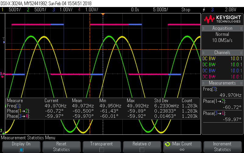
In another project, I’m using the two DACs in my F0 processor to produce two sinewaves with a precise phase shift. I was using the scope to measure the resultant phase difference and was a bit disappointed with how sloppy the results were, but it turned out it was because the scope was having to do an A-to-D conversion on each channel and compare the results. It’s a fairly high bandwidth scope but things were still slopping about. By enabling the Analog comparators and plumbing their outputs through to some spare GPIOs, I could confirm my phase shift was much more precise than the scope was clocking it at.

I thought I was generating them with a 60° phase shift. You can see in the pic below, the scope thought they were shifted by 60.5° with a standard deviation of 0.24° (Yellow to Green phase shift), but by using the Comparators to make the same measurement it came in at a much more respectable 59.97° with a standard deviation of 0.015° (Blue to Pink phase shift):

All that is a fairly long-winded way of saying if you want a precise timing indication of a particular voltage occurring, then staying analog will probably give you a better result than putting an A-to-D between the signal and the comparison. But it’s also possible the added precision doesn’t outweigh the pin/flexibility trade-offs.

1 Like

Not a direct answer to your question, and a lot of it will probably depend on good board design, but just using the Nucleo development board and jumper cables I wrote a program a while back that output a 50Hz synthetic sinewave on DAC1 (Blue trace) which I then jumpered across to ADC0 to re-digitise and I then got DAC2 to output the digitised results (Red trace) and here’s how it looked:

Incidentally, here’s the gist of the program. You can see the cpu is not involved at all in all those ADC and DAC conversions… it all happens autonomously in the background with DMA and timers while the CPU is burning cycles with nothing to do.


  // Put a 50Hz sinewave out on DAC1
  // Digitise it on ADC0
  // Output digitised signal on DAC2
  //
  // Connect PA4 (A2, DAC1) to PA0 (A0, ADC0) and probe it
  // Also probe PA5 (D13, DAC2) to see redigitised signal.

  snprintf(log_buffer, sizeof(log_buffer), "Hello world\n");
  debug_printf(log_buffer);
  
  init_sinewave();
  start_DAC();
  set_DAC_value(0);
  start_ADC();
  start_timer();
 
  
  /* USER CODE END 2 */

  /* Infinite loop */
  /* USER CODE BEGIN WHILE */
  while (1);


  /* USER CODE END WHILE */
2 Likes

Those 3 posts have probably saved me a few hours of wallowing through manuals - thanks!

Thanks @dBC, Lots of info there to take in. Currently the more I learn the more questions I seem to have.

You’re both very welcome.

Yes, been there and felt that. They’re complicated beasts and take some mastering, but once you do, you won’t look back. Even now there are entire subsystems I’ve never had cause to look at before. Today I found myself needing to use the internal RTC for the first time ever, so I’m back pouring over Reference Manuals and HAL API manuals to come up to speed on that.

Given I’ve only ever played with an F0 with a single ADC, I thought I better check if any of what I wrote above was true ;-). AN3116 is a pretty good high level description of the ADC features if you haven’t come across it yet. One spot where I slipped up is assuming you could sychronise all 4 ADCs. It looks like they synchronise in pairs so ADC1 and ADC2 can run together, and ditto for ADC3 and ADC4. And it appears at the time of writing that application note, they only had devices with 3 ADCs, but checking the datasheet for your F303 Paul, they do indeed pair ADC3 and ADC4 together.

That application note even uses calculating real power as an example of why you’d use simultaneous mode. The other interesting thing to note about simultaneous mode is that you fetch both ADC1 and ADC2 conversions from ADC1 as a 32-bit value. So my DMA description above (4 DMA channels x 16-bit wide) is not quite right for simultaneous mode (it would be if you were running all 4 ADCs independently). In simultaneous mode you’d use 2 DMA channels x 32-bit wide.

I haven’t confirmed yet, but packing the two 16-bit results side by side in a 32-bit word like that might lend itself to being just right for some of the single cycle multiply-and-accumulate DSP instructions found in the M4.

Thanks @dBC for the input. I’ve been reading through all the posts again trying to make sense of it all. Lots to learn.

Paul Burnell - Nucleo F303RE slightly slower, less SRAM but much more appealing ADC specs (4x 12 bit ADC’s, 40 channel potential on 128pin package or 22 on 64pin package, 18msps, 4x op amps, programmable gain or mid rail voltage).

@pb66 the F303RE certainly sounds better than the F401RE I picked up to test above.

Level based interrupts sounds useful.

Did you mean the F373, or is there a F303 configuration?

@dBC Where is the best place to learn about stm’s HAL layer? Do you have any good low level examples of using the ADC’s? Should we start by reading AN3116

Interesting reading through this post highlighted by @Bramco Change Timer clock source - Arduino for STM32

I did actually think I was talking about the F303 but I can now find no evidence to that effect so must of gotten them mixed up, easily done there so many different models.

I too would like to know more about this, more specifically I would like to know how using the stm32cubeMX for the HAL can be combined with using the Arduino IDE. It seems to be common practice going by the forum discussions but not something that’s explained very well, if at all.

I have found using the cubeMX easy enough and have found it can output files in various formats for use with several dev environments (but not Arduino explicitly) and there is also a generic “makefile” output, but then what?

I’m struggling to understand how the Arduino IDE makes use of those files.

I have used the Arduino IDE alone to upload sketches to the STM32 and monitor the serial output, but only some very basic stuff.

I have also used the cube programmer and the “flasher loader demonstrator” but I seem to be missing a bit of the puzzle to get any of these to work with any other bit.

The ultimate reference is the HAL User Manual, and while they’ve aimed for portability across the range, they do have a HAL User Manual for each family, so I invariably have:

“UM1785 User manual Description of STM32F0xx HAL and Low-layer drivers”

open on my desktop as I use the F0 family. You’ll want to replace that with whatever family you’re using. But it’s not really tutorial style. I’m not sure if anyone programs to it directly, it’s way too complex ;-). As it sounds like Paul has discovered, the trick is to use the User Manual in conjunction with their GUI tool STM32CubeMX. That tool lets you configure all the complexities of the ADC, DMA, Timers, interrupt controllers etc. in a fairly friendly way. The .ioc file it uses to maintain all your project settings becomes a vital part of your project “source code”.

Once you’ve defined all your h/w usage in the GUI, you hit “Generate Source” and it creates a source tree for your project which will include 99% of the HAL calls you need to make, already coded up and ready to compile. The code is full of sections such as:

  /* USER CODE BEGIN 2 */

  /* USER CODE END 2 */

which is where you put your stuff. Initially I figured I’d run the GUI tool once at the start of each project and then just edit the source (both my source in the sections above, and their generated source) from there on in, i.e. i was thinking I’d use the GUI to kickstart each project and then take over manually from there with the editor of my choice. But I quickly learned the true value of the GUI tool and now love it, so I now include it in the development cycle. If I want to change a setting on some ADC parameter, I go back to the GUI tool, change it there, save the .ioc file, and hit “Generate Code” again each time. There’s a vital setting to keep user code when re-generating. Here are the settings I use:

One big downside of including the GUI tool in your development cycle is it’s much harder to document a simple step-by-step guide to something like using the ADC. Almost all the work happens in the GUI long before you get near a text editor to work on the source code. If I just flipped you the source code, you’d be overwhelmed by the complexity (as would I) but you have to remember that the GUI wrote 99% of it.

I’ve just got myself an F303 board, the same as Paul’s, as I wanted to check out the maths performance of the M4 so it seemed a pretty cheap way to go. When I get a chance, I’ll use it to document the creation of brand new project, from GUI through to uploading to the board, and make sure it includes some low-level ADC stuff (well, low-level compared to analogRead())

That bit I can’t help you with as I don’t use the Arduino IDE for stm32 work.

Sounds like you’re well on the way. That “Makefile” option is new, and I’ve recently switched to it since updating my cubeMX. I won’t bore you with what I had to do previously to create a Makefile, but it was pretty tedious and involved python scripts.

There are a couple of bugs in the generated Makefile (at least for Linux users like me), but they’ve been reported in the stm32 forums, and have easy workarounds. Bugs aside, all you need to do now is type:

$ make
$ cp build/DSP.bin /media/dbc/NODE_F303RE/

I’ll include a bit on how to fix the Makefile bugs in my step by step example.

That second line is all you need to do to flash your new image into the target. DSP.bin is the output of my build. You’ve probably noticed that when you plug your Nucleo board into your PC it appears as mass storage device. It’s not a real mass storage device, but if you copy a .bin file to it, it will flash it into your F303 for you. No need for any avr-dude equivalent. Any computer that knows how to write to a USB mass storage device (i.e. all computers) can re-flash with a simple copy command, or even drag-n-drop to the device if you’re that way inclined.

To see the debug printfs, I just run up minicom and point it to the USB tty device that also appears when you plug in the Nucleo board.

Thanks @dBC that’s really useful to get an insight into your development process. I will take a look at the GUI tool and the user manual, I just opened one and there are 1700+ pages! that must have taken a lot of time for the authors to write.

I’ve been reading through the source code behind the adc_read_value function in the stm32dunio library https://github.com/stm32duino/Arduino_Core_STM32/blob/master/cores/arduino/stm32/analog.c#L553 and reading up on the commands line by line, I feel like Im starting to get somewhere. There are a number of tutorials and stackoverflow Q&A that help to make sense of it and the application note you suggested also gives a useful overview of the different modes.