STM32 Development

Removing R31 and adding a 2.048V voltage reference should be possible here

image

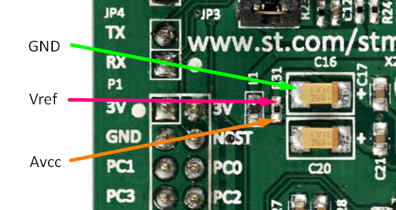
it’s beyond my knowledge to know whether C16 or C17 need removing/replacing, the data sheet certainly says a cap is required, but I do not know what the optimum values might be.

I guess the Vref pin would also need connecting to one end of a pair of identical resistors connected in series from Gnd so that voltage divider can provide the voltage ref for the op amp midrail at 1.024v.

The Discovery boards do not have the Arduino connectors, but that would not be an issue if we are making something with more CT’s, it can fit the Discovery conns.

The Discovery is a couple of quid cheaper than the Nucleo144 boards, and has a “STM32F303VCT6 microcontroller featuring 256-Kbyte Flash memory, 48-Kbyte RAM in an LQFP100 package” So whilst it has a smaller flash and SRAM, it does have all 39 ADC channels accessible and the ability to use an external Vref (by hacking the proto board).

http://www.st.com/content/st_com/en/products/microcontrollers/stm32-32-bit-arm-cortex-mcus/stm32-mainstream-mcus/stm32f3-series/stm32f303/stm32f303vc.html

I do not see any other obvious differences in the MCU (I’ve not checked every feature), the board however is radically different, it still has a STlink programmer, and it also has a compass, motions detector and gyroscope (not that an energy monitor has much use for any of those), but they might be fun to play with once the monitor is built :smile:

Obviously that is the ideal case. However, there’s a thing called “the real world”, and compromises are necessary. Everything depends on the application. I have previously suggested that we should consider using 0.333 V inputs (~ 1 V peak-peak), because there is a wide choice of c.t’s (and a precision v.t.) with that output. If the advantage of that outweighs losing 1 ADC bit (i.e. using only half of a 2.048 V input range) then that is the better choice. What I think needs to be done is to aim for a realistic minimum of distortions and aberrations in the front end, because that simplifies everything. Then compensate for what’s left (like we do with phasecal in emonLib).

We must not forget that the Atmel application note on which I think the design of the emonTx was based (AVR 465) did in fact use a programmable gain amplifier in the front end, designed for 1 V peak-peak from the burden resistor at minimum gain.

You might know this already, but in case not, there are a lot of different versions of ST-LINK. TN1235 lists the history of it all. Looks like you need version C or newer of that Discovery board to enjoy the features we’re currently using on the Nucleo: (debug comms port and USB mass-storage flashing).

Everything inside the c.t. that is frequency-dependent is a first-order effect only (no f2 or higher orders) so for the less than 1% changes that are the case for the majority of uses, then I expect the deviation due to frequency changes alone, at a reasonable fraction of rated current, to be that or less.

However, the transformer errors are due to reactive and resistive voltage drops in the windings and magnetising and core loss components of flux. The two components of the volt drop are in quadrature, but so are magnetising loss and core loss, so the overall effect is not directly related to frequency after all, especially at low currents when the loss components become more significant (because they decrease slower than the components that are related directly to the load current).

Unfortunately, without knowing the full details of the windings and the core materials, it’s impossible (and outside my experience anyway) to know exactly how a particular c.t. will perform.

I knew there were different versions and that the Nucleo has v2.1. But the discovery datasheet seems to say either a v2 or v2-B can be fitted, but that was back in July 2016, There doesn’t appear to be any obvious way to tell them apart, but I would hope a larger stockist such a s RS or Farnell to have the more recent versions, and I might even be tempted to call them first to confirm (if they know) now I’m aware. to avoid getting a “back of the shelf” old unit.

But if it’s the only way to test the front ends we are thinking of, it might be worth the pain of using an older STLink, or since most of us have a Nucleo, a few link wires and the STLink v2.1 of the Nucleo could be used to program the Discovery’s F303 if push come to shove. I wouldn’t let the programmer stand in the way of evaluating a better Vref and more ADC channels.

Here’s some low-end performance data I half-captured yesterday but didn’t get around to posting. This is with the calibrator set to 230V, 0.5A, 50Hz, 0°. The Preal numbers are surprisingly good:

CPU temp: 37C, Vdda: 3304mV
0: Vrms: 230.13, Irms:  0.67, Papp:  154.98, Preal:  115.12, PF: 0.743, Count:147032
1: Vrms: 230.13, Irms:  0.69, Papp:  159.18, Preal:  115.77, PF: 0.727, Count:147032
2: Vrms: 230.13, Irms:  0.72, Papp:  165.77, Preal:  115.37, PF: 0.696, Count:147032
3: Vrms: 230.14, Irms:  0.53, Papp:  122.34, Preal:  114.48, PF: 0.936, Count:147174

The lousy PF and Papp are all down to the noise that’s showing up in Irms and is also seen by the scope:


And that supports Robert’s suggestion of putting an LPF on all inputs.

What’s most surprising is that the net phase error doesn’t seem significantly different from what was calibrated away at 10A. I’m still running that same demo8 image which has the phase correction set to:

const int ADC_LAG = 269;             // ~4.8 degrees

With the calibrator set to 230V, 0.5A, 50Hz, 90° there’s amost nothing leaking into the Preal column:

CPU temp: 38C, Vdda: 3302mV
0: Vrms: 230.11, Irms:  0.68, Papp:  156.70, Preal:    0.36, PF: 0.002, Count:147006
1: Vrms: 230.11, Irms:  0.69, Papp:  158.93, Preal:    0.97, PF: 0.006, Count:147006
2: Vrms: 230.11, Irms:  0.73, Papp:  168.94, Preal:    0.60, PF: 0.004, Count:147006
3: Vrms: 230.11, Irms:  0.53, Papp:  122.35, Preal:  -14.03, PF: -0.115, Count:147007
1 Like

That’s not that far removed from what I found with my measurements. Of the 4 most recent c.t’s with a black cable and moulded plug that I tested, the range was 3.21° to 3.28° at 10 A, rising to 3.88° to 4.32° at 0.4 A, and for 3 of the 4 samples, the slope was remarkably consistent between 0.4 A and 80 A.
0.5 A is still above the point where the phase error starts to show signs of increasing. I couldn’t get reliable results below 0.25 A (that’s a bit less than 3 mV rms across the burden), so I’ve only got one point, the 0.25A measurement, where it is showing signs of increasing.

Nice. I guess I haven’t been paying enough attention. That’s a lot flatter than I was expecting for some reason.

That fits the description of the SCT013s Trystan sent me. And of course your absolute numbers aren’t directly comparable with my absolute numbers because you’re measuring relative to the signal, and I’m measuring relative to the output of the VT (with its own phase shifts - but hopefully constant at a constant 230V).

Here’s what I see at 0.1A (ignore CT4, I’ve removed it from the loop so I can test the high end without fear of blowing an input).

230V, 0.1A, 50Hz, 0°:

CPU temp: 38C, Vdda: 3304mV
0: Vrms: 230.04, Irms:  0.47, Papp:  107.33, Preal:   24.10, PF: 0.225, Count:147032
1: Vrms: 230.04, Irms:  0.47, Papp:  109.24, Preal:   24.12, PF: 0.221, Count:147032
2: Vrms: 230.04, Irms:  0.53, Papp:  122.01, Preal:   24.29, PF: 0.199, Count:147032
3: Vrms: 230.05, Irms:  0.19, Papp:   43.91, Preal:    0.55, PF: 0.012, Count:147031

230V, 0.1A 50Hz, 90°:

CPU temp: 38C, Vdda: 3302mV
0: Vrms: 230.07, Irms:  0.47, Papp:  107.60, Preal:    1.25, PF: 0.012, Count:147037
1: Vrms: 230.07, Irms:  0.47, Papp:  108.20, Preal:    1.33, PF: 0.012, Count:147037
2: Vrms: 230.07, Irms:  0.54, Papp:  123.76, Preal:    1.39, PF: 0.011, Count:147037
3: Vrms: 230.08, Irms:  0.19, Papp:   43.00, Preal:    0.57, PF: 0.013, Count:147037

I think the only sensible approach here is to ignore the noise riddled Irms/Papp numbers and compare Preal with what it should be: 23W in the resistive case, and 0W in the reactive. So for channel 0, arccos(1.25/23) = 86.88° Vs an ideal 90°, so about 3.12° different from what it was at 10A.

[EDIT] - the obvious flaw in that approach is that it assumes none of the noise is at 50Hz. The fact that the resistive reading is high (24.1W Vs 23W) tells us that some of the noise is at 50Hz, so I don’t think we can blame the entire 1.25W in the reactive case, on phase error alone… i.e we probably need to divide by a bigger number than 23 in the arccos() calculation.

Is that a software low-pass filter (LPF) or a physical LPF, I assume a physical LPF will add to the component count (more cost and more PCB real estate especially with 20’ish inputs).

I recall comments about a programmable gain amplifier (PGM) being added to each input to allow lower voltage CT’s to be used (rather than or in addition to a lower Vref) but I’m guessing all those opamps would also be costly (comp’s and real estate) too.

Not saying the’re bad idea’s, just checking I understand what is being suggested.

Although the newest SCT-013-000’s might be flatter at 22R or 33R, there are hundreds and thousands of CT’s already out there and we would like to accomadate a wider range of CT’s. Since we know CT’s behave better with lower burden’s, achieved by using a lower Vref, are the comments about the latest SCT-013’s suggesting we stick with what we have?

IMO, if the MCU and PCB have the provision for an external Vref, it can be bypassed if it’s not needed/wanted, but once we commit to a MCU or PCB layout that prohibits a lower Vref (like the ST dev boards) we cannot explore or pursue that avenue any further without going back to the drawing board and accruing additional (PCB tooling?) charges.

Even if we are not able to get a software LPF solution working for the first release, we might be able to continue development if the initial MCU/PCB choices permit it.

The longevity of this design will come from accommodating choices and thinking further ahead. Even if rev1 has Vref and Avcc linked (and 22R’s fitted?) to predominantly suit the latest SCT-013-000’s, we then have boards we can hand modify for development and eventually a minor change of component values/population might accommodate a much wider range of CT’s.

Adding op-amps for PGA’s and/or fitting LPF’s can be done on the front end sub boards, but the Vref must be done on the main MCU board so making it definable is a core decision, even if we then choose to set Vref to 3.3v.

This is why I keep suggesting a proto board, think of the Nucleo or Discovery as our monitor’s (temporary) main MCU PCB and the proto shield(s) as our 1st front end, for the cost of a few cheap PCB’s (which do not need fully populating initially) we can try various approaches, we might even find several methods that work for varying applications (that is the idea behind the modular approach) but if we try to go to straight to press with one design partially tested and focus on “the norm” we will undoubtedly not have used the most flexible setup on the main MCU board and block certain avenues of future development.

I accept that the link wire’s is not the best idea, perhaps we can just make a board that breaks out all 39 adc’s to 3.5mm sockets and each has a footprint for VT input (voltage divider instead of a single burden) that way we can populate any input for CT input by using a 0R link (bit of wire) to “convert” the voltage divider circuit to a burden OR for a VT by using 1 to 3 “barrel plug to 3.5mm socket adapters”.

Come to think of it, we could even use some of the “IoTaWatt Direct 3-phase adapter kits” whilst prototyping if that’s easier.

1 Like

And we really should have an anti-alias filter on every input. You cannot do that in software.

1 Like

Yep, you won’t find a single ADC (or energy IC) datasheet that won’t tell you they’re essential. I was actually using the terms LPF and anti-aliasing filter interchangeably.

The recommended approach is to filter the signals once they get to the board, and from there on in, be extremely careful with board layout, trace length, ground planes etc. between there and your ADC. I was initially a little nervous about the modular approach and what it will mean for noise, since these are analog signals where every mV counts. With a 2V Vref, 1/2 an LSB is about 244uV, but provided you put the LPFs on the main board, right near the ADC inputs it could well be ok. These signals have already travelled through a pretty harsh environment to get to the box and the “modularity” hopefully won’t be any worse than that.

I think you need to draw a line somewhere, and put your LPFs there. Everything to the left of the line is noisy, and everything to the right of the line involves extremely carefully placed short PCB traces.

1 Like

I appreciate the point about the signal level, I think I expressed that in a roundabout way early on when I wrote that any connector was a potential problem, but I feel that careful design - appropriate filtering, shielding and screening - should be able to take care of that. I’ve got to point out that professional audio equipment operates with noise levels approaching two orders of magnitude better than that, so better than ½ LSB should be feasible.

Are they mixed signal though? It’s when you’ve got all that high speed digital switching going on right beside your mV analog signal traces that it can get nasty. Actually, they probably are these days… they all seem to be full of DSPs.

Indeed, that’s why it needs to be thought through at an early stage with the physical arrangement given at least as much attention as the electronics.

Analog Devices have a lot of good stuff. For example:

http://www.analog.com/en/analog-dialogue/articles/staying-well-grounded.html

While investigating noise at very low Irms settings I discovered quite a bit of it was actually caused by a rounding bug, and low precision in the FP maths (float instead of double). Unfortunately the M4’s FPU only does single precision, so once you go to double it’s all done in s/w. This was a huge hit to the data-ready ISR which fires every 6.8msecs. It went from taking 1.05 msecs (to process 200 400 V,I pairs in single precision) to 4.24 msecs. So instead it now does all the ISR maths in int64_t which brings the ISR runtime back down to 1.09 msecs while still enjoying full precision.

The final crunching of the numbers for display uses double precision, but only happens every 10 seconds so doesn’t really matter.
txshield_demo_9.tar.gz (896.1 KB)

Thanks @dBC, I have updated the stm32tests repo with tar 9, the diff can be viwed at emontx_demo_9 · stm32oem/stm32tests@e816d48 · GitHub.

1 Like

How much does that affect your thoughts on the LPF?

I agree it would indeed be better to have the connectors on the “dirty” side of the filter, but I do not think it’s all that feasible to have <30’ish filters in close proximity to the MCU and including LPFs for every input on the base board may be cost prohibitive. It means even users that (for example) get an stm monitor for pulse counting alone, will be paying for the ADC input components. The same applies to the protection diodes and resistors, I’m inclined to think they should be in place for all adc inputs on the base board so that “3rd party” front ends are less likely to damage a stm monitor if no protection is included on the front end board, but that also bumps up the component count, cost and pcb size for every user.

The cost or space may be less of an issue than I’m allowing for, I’m still unsure what options are being discussed.

What would a (anti-alias filter?) LPF look like in our application? are we talking about passive components or something active using an opamp?

Only mention “opamp’s” here as I believe it was mentioned before in this context (assuming I haven’t got my wires crossed), if an opamp is used, can this be combined with the PGA circuit or are we talking about 2 opamps per input?

Another question about the LPF, will it impact the phase error? Reaching back into the depth’s of my memories of when I used to build speaker systems, I recall using 2nd order passive x-overs (LPF’s and HPF’s) so that the 180° phase error could be easily compensated for by inverting the output wires, is that relevant here? I assume an active solution would not have such an impact.

Would the components used be specific to either 50 or 60Hz? Would adding an LPF reduce the input’s flexibility to be used for other things?

Also, would increasing the sample frequencies help at all here by reducing the need and/or moving the LPF frequency to widen the “useful” range.

Just a simple first order LPF would suffice, so 1R and 1C per input… a small price to pay!

Yep, about half a degree at the fundamental for typical LPF choices in energy monitoring applications. That’s why you should always put the exact same filter on all your inputs (V and I)… that way they all get shifted together.

Nope, one size fits all.

Once you’ve chosen your filter parameters it would put an upper limit on the bandwidth of interest (the whole reason you do it), so you wouldn’t one day be able to use the input to sample a 1MHz signal. Provided you’re happy to lock in a bandwidth limit suitable for measuring 50/60Hz power (so somewhere in the 4 to 10 kHz range depending on how much harmonic power you wanted to measure) then no, it wouldn’t get in your way.

Nope, every ADC application needs an anti-aliasing filter. At the low frequencies we’re dealing with a simple first order LPF suffices, at higher frequencies, you’d probably need to go for a more complex filter.

Here’s a good little primer on LPFs: Passive Low Pass Filter - Passive RC Filter Tutorial

2 Likes

Thanks, that clears up a lot of questions. I was imagining an inductor rather than the resister. Is the LPF resistor likely to replace the 1K input protection diode or do we still need both?, needless to say I haven’t attempted to calculate what values we might actually arrive at.

If we go for a MCU with 39 or 40 adc channels I expect we could tie in plenty for AC (50/60 Hz) and still have a few left over “just in case” of more exotic applications.