ESP8266 WiFi power monitor

I noticed others working with the ESP8266 processor, and wanted to share my device which is working but has a list of improvements that I’d like to make before calling it anywhere close to done.

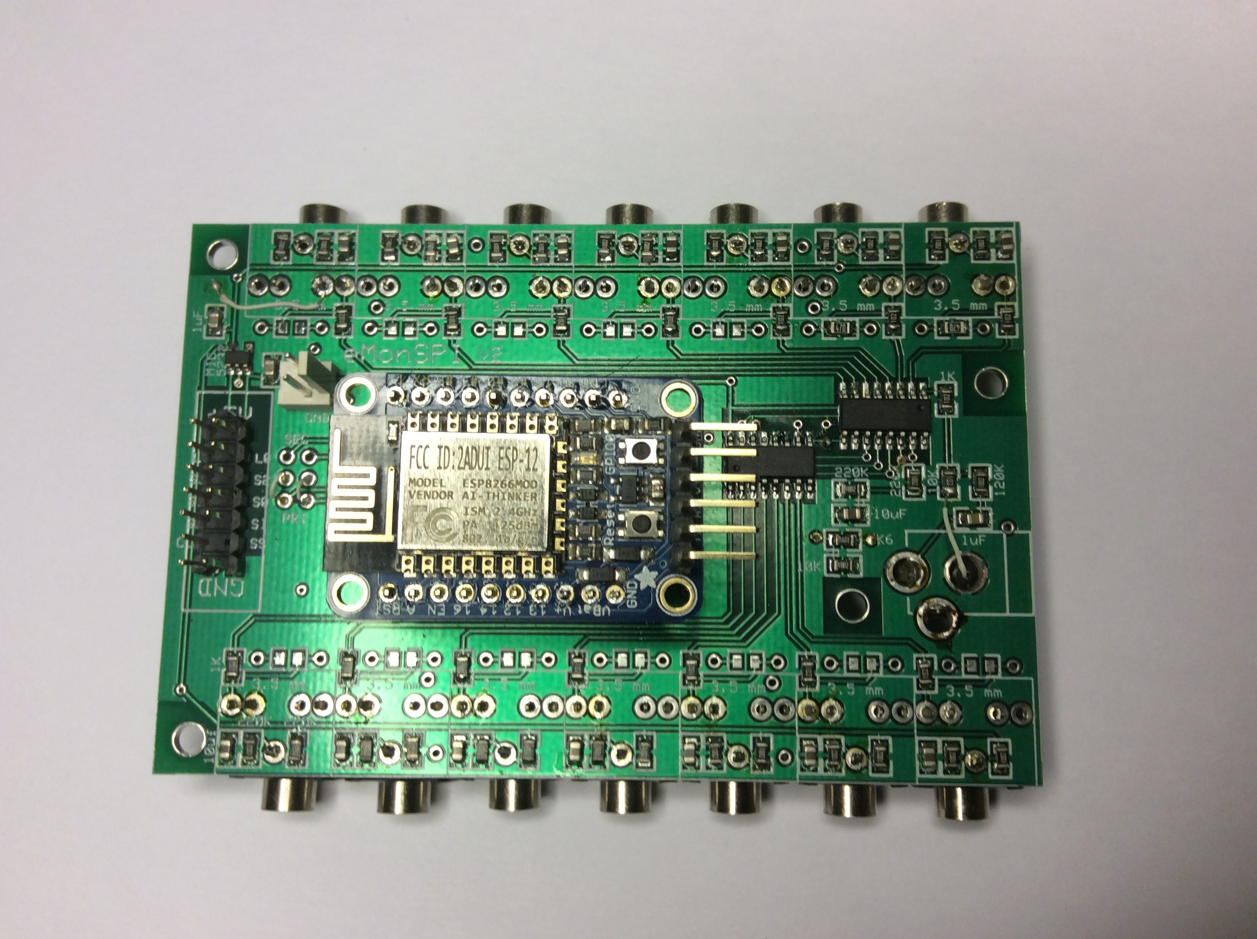
I’m currently using the Adafruit unit with the Arduino IDE as they document. The board uses a couple of MCP3008 10bit ADC’s to do data acquisition. The ESP reads them over SPI at 2Mhz for a sample rate of 347 voltage/current reads per 60Hz cycle. The 80Mhz 32 bit processor is in a whole different league from the Arduino. Tons of floating point calculation won’t slow it down.

I transmit the accumulated power to the EMONCMS cloud at 10 second intervals using the onboard WiFi, which seems to work very well. There is software available to facilitate configuring the WiFi network, and it has the capability to work as a server as well to add a configuration and/or display app.

Right now, I’m trying to deal with some unique challenges that arise from the high sample rates. The plus side is that there seems to be no difference in results when sampling one cycle vs multiple cycles, so the whole 14 channels can be sampled and processed in about 350ms. The down side is that the phase shifting in both the 9V AC voltage sense transformer and the various CTs have become a significant factor.

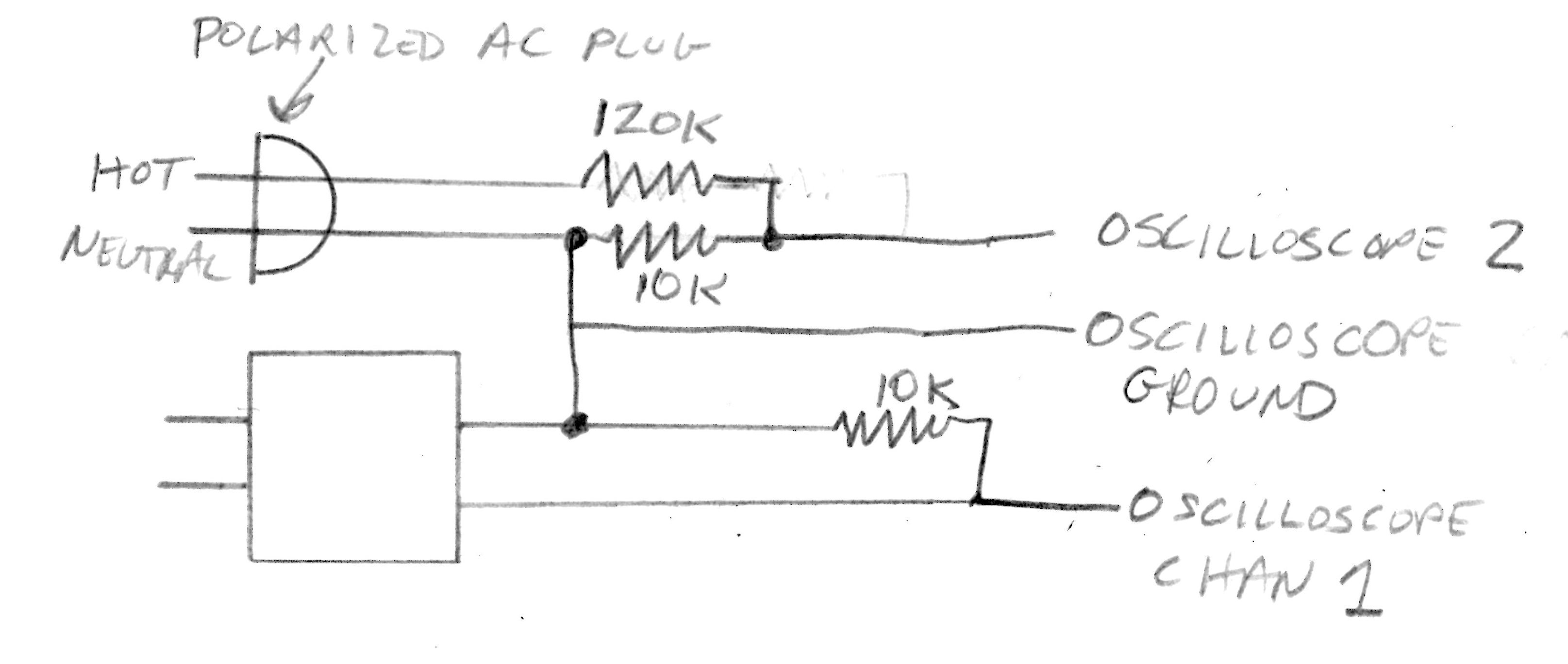
The samples are at just over 1deg while I’ve recorded what I think are phase shift errors of 10-19 degrees. I have read Robert Wall’s discussion of the SCT013-000 and the 4-8deg phase shifting there. I’ve also measured what I think is a 6deg phase shift in the AC voltage reference transformer. I looked at the phase difference between the voltage and current readings and found it to be about 14deg. That’s the number of samples between the sample pairs where each crosses zero when looking at a purely resistance load. Robert - any thoughts? It amounts to about a 2% reduction in real power. Obviously, no impact on RMS power.

Back to the ESP8266 in general - I’m going to try to add a decoupling transformer and power supply so that I can run the whole thing off the 9V AC reference. Right now I have 5V from an external supply. I’m using a 3.3V regulator for the ADC circuits (the ESB HUZZAH has it’s own) and it seems to be stable within the margin of error of the phase shifting and cheap CTs that I’m using.

I’ve been very pleased with the prototyping boards from ExpressPCB. I’m using their 2.5x3.8 standard size, and get three delivered, with solder mask and screen for about $70. Quality has been excellent. The application is a lot different from Eagle, and seems easier to manage for what I am doing.

I’ve been concentrating on the power meter application, and not looked at much of the other stuff people are doing, but obviously this processor has the capability to easily add temperature (one wire or 10K) and any number of input/output switches - and probably just about anything else. Right now, board real estate is the governing factor. I have designed it so that two can be coupled for a total of 28 power channels. The second board would not have an ESP8266 but attaches with a ribbon cable to the header.

That’s all for now. Looking forward some discussion and advice from people who might know more about the the phase shifting issues. Cheers.

7 Likes

Looks really interesting, and 14 channels, excellent, something I have had in the back of my mind to do for a while now looking forward to more updates.

Timing the zero crossing is actually the wrong approach, the best (and of course hardest) way is to do a FFT on the two waveforms and derive the phase of the fundamental component.

First, you need to choose the order that you read the samples in order to use the timing difference to minimise the apparent phase shift. Then, what you might need to do is delay processing one or other of the samples for a given number of samples, again turning the phase shift into a timing shift. FInally if necessary (and it might not be if you can hold up that sample rate), you do the interpolation - and try to do interpolation rather than extrapolation, it leads to smaller inaccuracies. Also bear in mind that you phase shifts aren’t constants, and will vary with voltage / current.

What is rms power? There is average power, but rms power is meaningless. I think you meant apparent power (VA).

Beware the transformer impedance. If you’re not very careful, you’ll put a significant dent in the waveform you’re measuring for the voltage. There are pictures in the old forums showing the effect (simulations using the measured parameters of the a.c. adapter and the emonTx V3 circuit).

What would be really interesting for the European market is a version with three voltage inputs for those people - mostly in mainland Europe - with 3-phase supplies. I think there’s a market there that Megni is missing out on. Would I be right in thinking yours is 2 V + 14 I?

2 Likes

Robert, thanks for the quick reply.

I guess what I was looking for is some kind of validation that my observed combined shift is a reasonable observation, and that correcting is justified. Even if I knew the exact phase shift of the two inductive components, as you point out, the shift in the CT varies with current. So my goal would be to mitigate a 10-20deg shift down to around 1-2deg so as to achieve an overall accuracy within 2%.

Dealing with the shift in software is pretty easy. Turns out that the limiting factor in acquiring the sample pairs is the SPI implementation in the ESP. The actual data rate at 2Mhz is what you would expect at 1Mhz. So there’s plenty of time available. What I’ve done is to actually save all of the VI pairs in memory for a cycle+, and process them later. With this technique I can actually “slide” the current over the voltage by simply adding a constant to the array subscript. As you point out, since I can sustain the high sample rate, interpolation isn’t necessary.

I measured the AC voltage transformer shift at about 6deg with an oscilloscope using a voltage divider on the actual AC line and the output of the transformer. The AC line crossed zero about 280us after the transformer output, so I interpret that as a 6deg leading shift (60Hz). So the CT must shift in the opposite direction 8deg when I observe a 14deg combined shift. My question is why does the AC transformer lead and the CT lag? (I may have that terminology backwards, so straighten me out). [quote=“Robert.Wall, post:3, topic:1692”]
What is rms power? There is average power, but rms power is meaningless. I think you meant apparent power (VA).
[/quote]

You’re right. I was loosely calling the product of RMS voltage and RMS current RMS power. I’ll try to stick with apparent power.

Looking at it with an oscilloscope, the AC signal before the uncoupling transformer seems to be OK, and my intention was to use that for the voltage samples. You are right in that the uncoupling transformer output is both phase shifted and distorted, so I would use that for the power supply. Actually, there isn’t much of a downside to just staying with an external switching 5V power adapter.

What you see in the picture is 1V + 14I. There’s one unused channel on the second ADC. The standard size PC board would only accommodate 14 CT plugs. But you’re right in that another voltage input could easily be configured to the unused channel.

I seem to recall that a third phase can be derived electrically from the other two, so I assume that could be done mathematically as well, but it would probably be easier to just go with 3V - 13I for a three phase monitor. The way this device is scaled, you could add any number of additional boards for more CTs. I’ve run mine with 28 CTs - no problem. The phasing might become more of an issue though with three phase voltage sensing and three CTs. If you want to pursue this, I think that with a fast processor like the ESP, it’s possible to roll your own SPI with an external clock and to read three ADC’s simultaneously. SPI has discrete MISO lines. I’ve explored this a little as a way to read the voltage and current simultaneously with the previously mentioned extra voltage sensor on the unused channel of the second ADC. I was also looking at a more expensive 12 bit ADC ($7) that can be set up to read any of the inputs quickly into a FIFO.

I

Wow, very impressive. Nice work :thumbsup:

Is the unit open-source? Have you posted the the design files and source code anywhere?

What software are you running on the ESP? I wonder if you would find EmonESP useful to post to Emoncms?

Have you calculated the source impedance of your analog signals? The MCP3004/3008 datasheet goes into a fair bit of detail of what’s need at various clock speeds, but it looks like at 2MHz you need a fairly low impedance source. I’m wondering if some of your apparent phase shift might be caused by the sample-and-hold cap not being given sufficient time to charge?

That’s a big difference that I found between using something like an Arduino 2560 with 16 channel ADC and the MCP3008. I started out using 220K resistors for the bias voltage dividers. As I increased the SPI speed, the measurements sagged. A lot.

Not being an EE, I spent a lot of time figuring it out trial-and-error. Mostly error. What I’ve come up with is using 10K resistors for the bias voltage dividers. Draws a lot more current than the 220K’s but on balance, it’s only about 2-3ma for that portion - A couple of orders of magnitude less than the processor when it’s doing WiFi. The most obvious indication of problems is when the average ADC reading (the offset) is not very close to 512. All of the channels run at something between 510 and 512.

What seemed to be key was using 10uf caps on the ground side of the voltage dividers, as opposed to the 1uf that I started with. I speculate that they help provide the current needed to charge the sample capacitor in the ADC. I also put 1K resistors at the ADC inputs for what I hope will give them a little protection against voltage spikes. Using 470ohm resistors, or none at all, makes no measurable difference.

The most stubborn problem was the AC reference circuit. I ended up reducing the voltage there with a 10K/1K voltage divider. 100K/10K didn’t work and sagged a lot like the CT channels.[quote=“dBC, post:6, topic:1692”]
I’m wondering if some of your apparent phase shift might be caused by the sample-and-hold cap not being given sufficient time to charge?
[/quote]

The SPI bus speed does not seem to have any measurable impact on the phase shifting, and the 6deg phase shift of the AC transformer was measured with just an oscilloscope.

Thanks Glyn. The learning curve for all of this stuff is overwhelming. I have a Github account, and do intend to post everything as open source. There’s a fair bit of work to produce a new board, clean up the code, and add a configuration/calibration capability through a web browser (the ESP is already providing WiFi configuration).

Today I got one of those cheap “development” ESP8266 boards from China ($3.99 + $99 postage). Hooked it up and it works just as well as the Adafruit Huzzah, in fact, has it’s own USB so don’t need the FTDI anymore. The Adafruit was nice, but the shipping is the killer - $12+ for a $9 part. So I have to change the board for this new larger form factor. The good news is that it plugs into headers so I can us the real-estate underneath for other I/O (on-wire, switches, 5-20ma etc.)

I programmed it using C++ with the Arduino IDE as modified for the ESP.

Right now, I’m uploading my household circuits and mains to the EmonCMS cloud, so I’m very much interested in making it part of the effort. In my opinion, the biggest potential will be in the ability to configure the thing from a browser.

3 Likes

Speculate? Nope, that’s exactly what happens. When the multiplexer closes on that channel, a chunk of charge gets transferred from the bypass capacitor to the S&H capacitor. Q=CV is a constant (until the bias resistors replace the charge), so knowing the capacitor values, you can very easily calculate the voltage drop.

You might consider using an op.amp. to supply the bias mid-point. That should have a very low impedance - a few tens of Ohms at most - so very little voltage drop, and it’s economical too with 14 inputs all fed from the same place. Search the old forum if necessary.

I did try using a 1.5V regulated supply for the bias. It worked pretty well, except that when a few channels are busy, the noise starts to affect the low reading circuits (probably all of them but noticeable only on the very low circuits).

Are you saying that the design has problems or just offering another alternative? I did fit up a board with 1K voltage dividers, and it seems to work the same as the 10K’s, even with 1uf caps. Two channels, with 10K/10uf and 1K/1uf, with identical CTs clamped to the same load seem to produce the same results. Can’t say that for 110K or 220K.

For 3 or 4 inputs, the op.amp. is overkill. But for 14, I’d consider it. It removes 26 resistors and 13 capacitors. Maybe you had a noisy regulator - some can be, and op.amps can oscillate to if you get it some stray feedback capacitance in the wrong place.

You’ve probably figured out that this is probably my weakest area. I’m a software guy and had a lot of experience working on new computer design over the years, but there were real hardware engineers to do this detail and… it was pretty much all digital.

So i’ve spent a lot of time trying to be conscientious and making sure I have validation that the data collection is reasonably accurate for a consumer device. My current biggest issue seems to be the phase shift issues that are more relevant to this high sample rate design.

I don’t know anything about op-amps. I could come up to speed, or I could find somebody to help me (you?) but I first need to understand this is a problem.

The cost of the resistors and caps are negligible. The technology is pretty much the same as all the EmonTX schematics that I’ve seen. So can you be more specific about the problems that the op-amp would solve?

I’ve read a lot of very useful stuff in this forum authored by you. I’ve got a lot of respect for your experience and knowledge in these areas, but I need to know if there is a real problem or just a discussion of alternative designs that would produce the same results.

Looks very nice! Just what i was looking for :slight_smile:
I would like to monitor up to 41 CT sensors, so your stackable solution looks very nice!
Looking forward to find its designs!!

The big advantage of the op.amp. is that every input can share the same bias source, and it should exhibit a lower impedance, which should be good. ‘Should be’ because there still needs to be some means of protecting the ADC input if the input is over-driven (for a CT, that could be a downstream fault).
All inputs sharing the same source might not be a major advantage for you, but it does mean that you can filter just one input to determine the bias offset, and then a simple subtraction with no further ado will suffice for every channel. With a lower performance processor, that’s a big advantage.
Don’t forget that the cost is not the bought-in cost of the additional components, it’s the extra area that they require and physically putting them on the PCB, then testing them too.
The point about lower impedance being good means that you’re less likely to see errors arising from charging the sample & hold capacitor. The AVR spec sheet lays down a maximum source impedance (and I don’t expect it’s unique there), the inference being that a high source impedance will cause the voltage being measured to dip (or more correctly, change) as the source charges or discharges the S&H capacitor. That’s the effect you rediscovered when you had an insufficiently large capacitor. So with an op.amp. bias source, the current to charge or discharge the S&H capacitor comes from the supply via the output stage of the op.amp, rather than as a transfer of charge from the bias decoupling capacitor.
Finally, as you alluded to earlier, the op.amp. must be quiet in order not to inject noise into the system. You can of course get noisy resistors and capacitors as well as noisy op.amps.

Which you choose is a matter of weighing up the advantages and disadvantages of each, as you perceive them.

That’s a pretty good rundown of the issue as I saw it as well. When I used the voltage regulator, I fed it into the unused ADC channel directly to read the bias value. But with the 10K resistors, I get midpoint ADC readings of 510-512. Some of that is probably due to variation in the actual resistors, but that explanation alone would suggest 511-513. So I’m probably losing one ADC count. That’s the specified accuracy of the ADC, so I’m not losing sleep over it. With the voltage regulator (pretty decent one) I saw maybe 1 count variation with no ADCs, but while running with a few active ADCs, an idle channel would bounce around 3-4 ADC counts. Not good. Moreover, it didn’t seem to correlate with the AC phase, although that was just a naked eye observation of the numbers and not a true regression.

More importantly to my way of thinking, is that whatever the depression in the bias voltage is, it’s probably the same for each measurement, and as long as I take care to determine that value statistically, should be good.

There are three points in favor of resistors that I recognize:

  • Its a simple solution from my perspective.
  • As long as the bias is derived by splitting the AREF voltage, the bias value will be immune to noise in the AREF circuit. (there probably is a way to peg an op-amp to a reference off AREF as well)
  • The CTs sit on top of the bias voltage, and any contact to ground would effectively short the bias on all of the CTs with a common bias supply. With resistors, it simply dumps AREF to ground through a 10K resistor - 330ua.

So I’m going with what I’ve got for now. Any additional thoughts about the original phasing issue? Sliding the current current samples to be in phase with the voltage seems to be more accurate, but I’d like to understand why the AC transformer and CT seem to work opposite (lead and lag). Or maybe the CT is just like 20 degrees out and the 6 deg transformer nets to 14? That doesn’t match your measurements. This situation was measured on a YHDC STC013-030 - basically an SCT013-000 with an internal 62ohm resistor.

Thanks,

I haven’t measured the SCT-013-030, so I can’t comment, but I think it should be between the SCT-013-000 with a 22 Ω burden and the same with a 120 Ω burden, but closer to the 22 Ω curve. Also, I haven’t measured any a.c. adapters other than the UK ones, so I’ve no idea how your transformer behaves. Unless you have a means of accurately measuring either the voltage or the current transformer’s phase error, you’ll never know how the difference is made up, all you can know is the nett difference. And remember, I test at 50 Hz. The 60 Hz errors will be different.

I think we’ve got something to work with here.

See if this makes sense. made up a power cord with a voltage divider and plugged it alongside the AC adapter:


[ DON’T DO THIS - THIS CIRCUIT IS POTENTIALLY DANGEROUS - Moderator (RW)]

When I look at the two traces on the scope, channel one (the AC adapter) crosses zero 280us before channel 2 (the line voltage). My device presents an 11K load to the AC adapter, so pretty close there.

One 60Hz cycle takes 16666us, so I get a phase shift of 360 * 280 / 16666 = ~6 degrees. Not sure of the terminology, but I’ve been saying the AC adapter leads the line voltage by 6 degrees.

I suppose I could do something similar by scoping the VT against the same line voltage probe with various load on the AC line. Does this make sense?

Before you think any more about that circuit, stop and work out what will happen if something goes wrong, for example the neutral falls off outside your house.

The consequences barely bear thinking about. You’ve said you’re a software guy with not too much knowledge of electrical engineering, so quit while you’re still alive. You’ll have a neutral-earth fault and all the current that was carried by your neutral will flow through your 'scope lead to ground. and when that fails, everything is live to line.

3 Likes

Revisiting this question from a few weeks ago, there have been some new developments. I’m actually running the MCP3008s at 4MHz now, and as you point out, the sample-and-hold (S&H) cap needs a really low impedance source to work at that speed under “normal” conditions.
Even with 10K voltage dividers, I had quite a bit of sag running at 2Mhz. I came upon a software solution…

The datasheet explains that the S&H period is defined by the rising and falling edges of two specific CLK cycles in the SPI transaction. In another section, the datasheet recommends a methodology to program the SPI transaction when using a MCU where the transaction has to be in byte (8 bit) multiples. In that scenario, the S&H defining clock cycles are embedded in one of those bytes. You see where I’m going with this…

The actual SPI transaction is 17 bits. In a 24 bit stream, it is defined as the first “one” bit (the start bit) and the 16 bits that follow. They suggest right aligning the transaction, padding with seven leading zeros and the start bit in the first byte. You can shift the whole transaction left 4 bits so that the S&H period is defined by two cycles that straddle the first and second bytes. If you then separate the sending of those bytes, you can effectively make the S&H period any length you please. In my case, the natural latency between sending one and then two bytes seems to be enough to satisfy the S&H cap with my higher input impedance.

Just a heads up that the project direction has changed relative to scaleability. The next generation uses a NodeMod 0.9 development board ESP8266. These things are available for less than $5 from China and $8 or so from a US re-seller. It doesn’t make a lot of sense to gang a bunch of boards together to use one processor.

So in the case where you want to monitor 41 circuits, I would say it would work better to just use 3 of these devices, each independently sampling and sending their 14 channels over WiFi. A single AC voltage reference can be split to service all three, and the device runs on the USB power to the NodeMod boards, so power can come from a multi-port USB brick with three micro-usb cables.