The way this design has settled out, you can use any of the CT channels as a voltage sensing channel by adding a capacitor and two voltage splitting resistors externally. The resulting circuit would be identical to the “voltage” channel that is hardwired on the board. Associating the appropriate voltage channel with the various CTs would be trivial in software. With that in mind I’ll keep the voltage reference channel to an easily modified variable.
Can you just share the voltage reference by connecting the input pins on the nodemod’s and the voltagesensor? Or is an other connection required?
The voltage reference is read by an Analog to Digital Converter ADC that is not on the NodeMCU board. While I think it would be possible to interconnect all of those on-board-signals, it would require that they also have many other things in common like ground and ADC reference voltage. Also, given that these devices typically live near electrical panels and a lot of high-voltage AC wires, noise picked up from the interconnect wires could degrade the accuracy considerably.
The simplest and easiest way will be to split the AC wall plug into three 2.1mm power jacks.
Got a new prototype board and populated it. Working very well at a little over 63K samples/second. WiFi connection is solid. ADCs seems to be reading well within the margin of error of my Fluke 175 true RMS meter. Now I need to develop better calibration data for the CTs.
This version accepts the inexpensive NodeMCU 0.9 ESP8266 (about $6 US). It’s powered by the micro USB port. Uses the Arduino IDE with C++. I added a shunt voltage reference on the unused ADC channel (2.5v 0.1%) so the device self calibrates everything but the AC voltage reference. Also added is a micro-SD slot to log the power on board in addition to or instead of the WiFi export. An 8Gb SD card would hold a few decades of power logging at 10 second intervals.
Any of the 14 channels can also be used for 10K temperature sensors or standard 4-20ma output sensors. Build cost is under $40 at qty 3, assemble yourself. Mostly surface mount (way easier than thru-hole once you tool up a little).
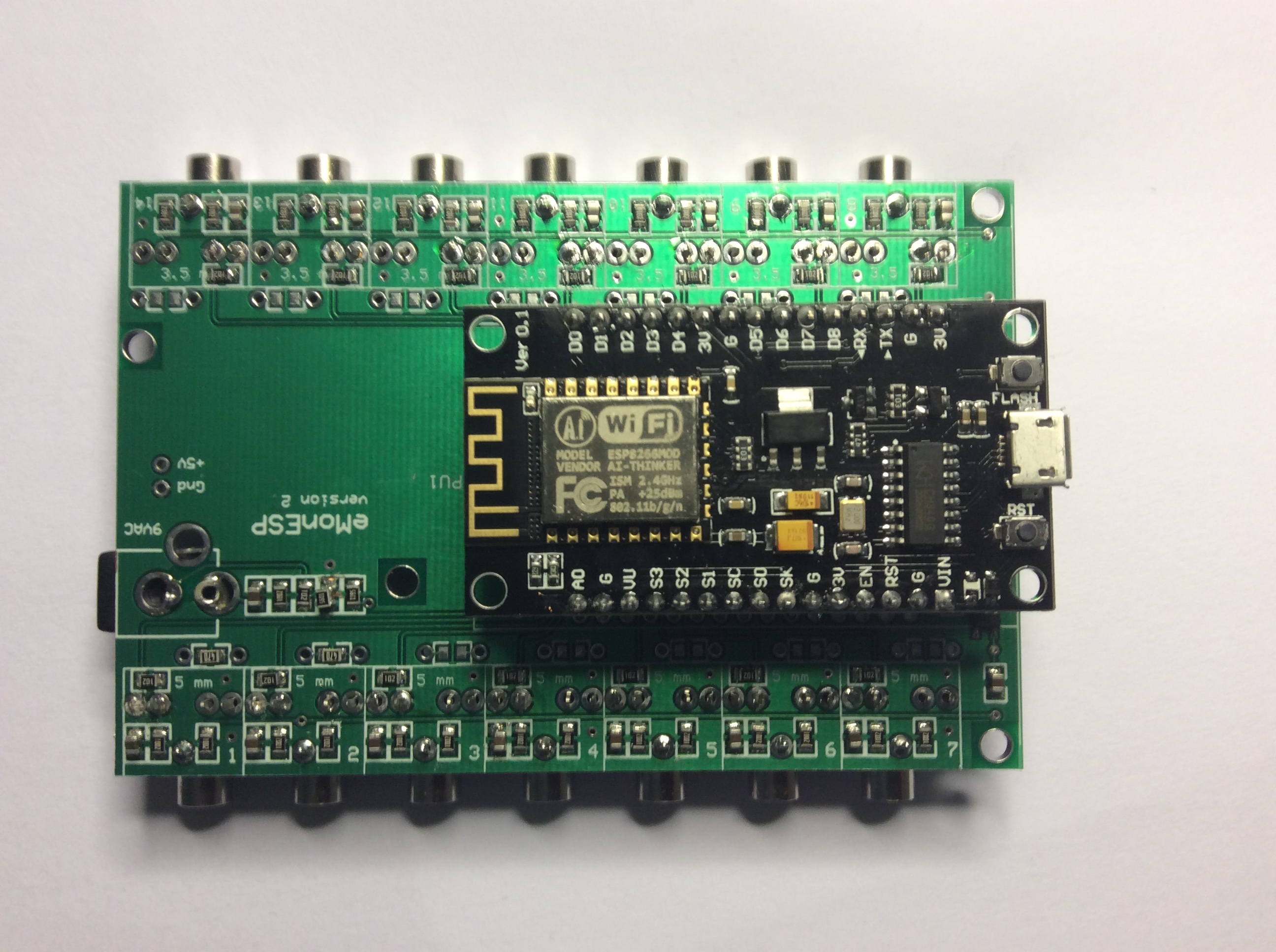
The ADCs are under the MCU board, leaving a lot of space for additional sensor/output hardware.

I’m working on putting the schematic and board on GitHub as well as the code. Also, there are still a few minor problems with the board that I had to rework. They will be fixed in the next version. I’ll also be removing the eMonESP logo as I see that the founders of this project are using that name for a version of their product that uses the ESP8266 as a WiFi add on.
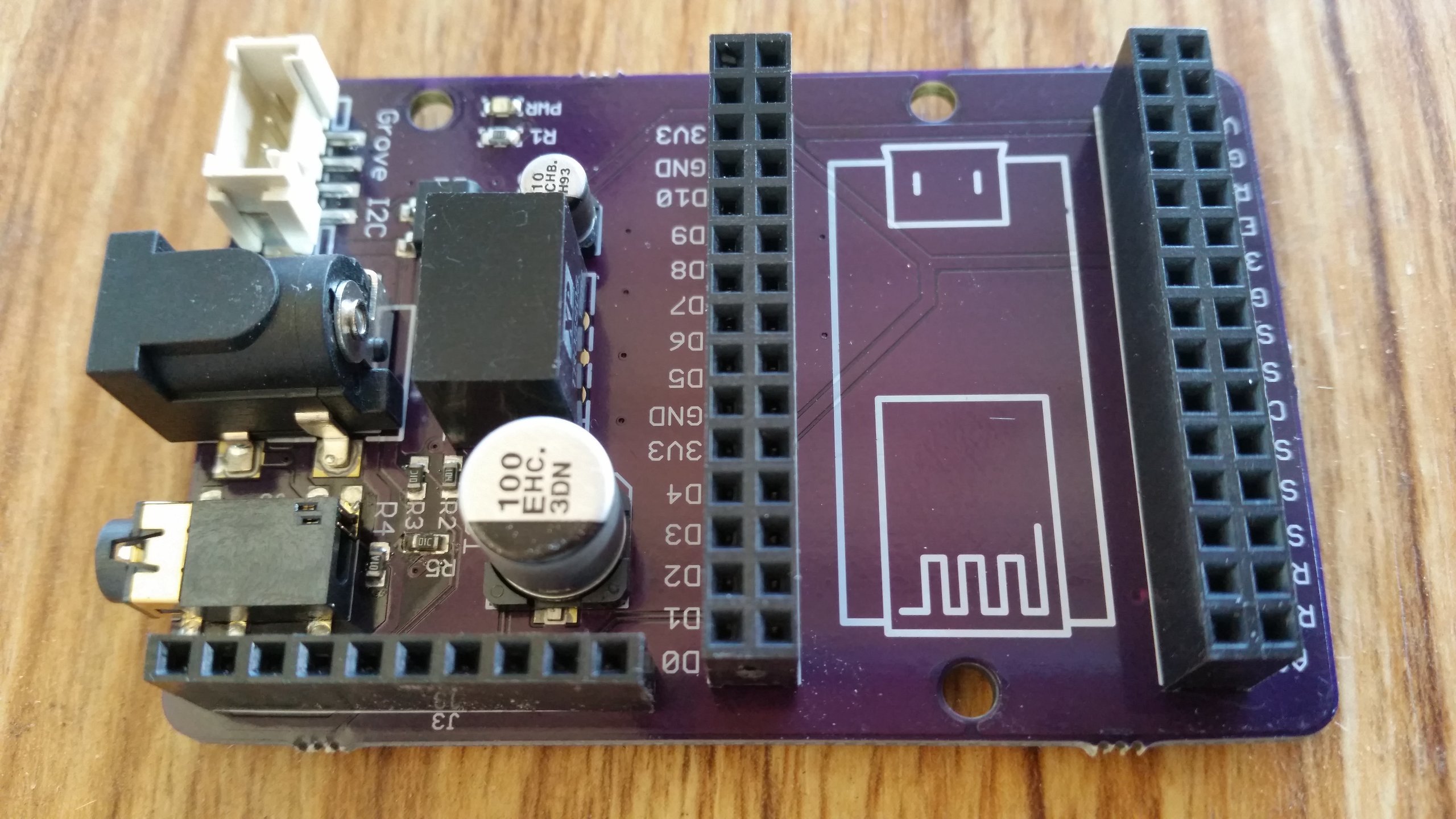
Great to see so many channels and a decent SPI ADC in use. Would love your design files to hack around and apply my experience with using I2C ADC’s (much slower) . I can recommend a usability change for the NodeMCU based design, add a double row of headers to be compatible with the different variants in the market. See my design below:
I’ll look into that. I understand that the NodeMCU 1.0 is narrower. I didn’t know it had the same pinout. That being the case, It would make sense to use the double headers. I’d have to tighten up the traces a bit to squeeze the ADCs in there, but I think it’s doable.
I’ll be publishing the schematics and PCB files, hopefully within the next month. But here’s the schematic. I’ll make the code available on my blog soon.

10/29/16 Note schematic has changed to version 2.1. Pinout on the microSD was changed.
I source my connectors from a certain shop on aliexpress for large quantity use and from RS-Online or Element 14 for prototyping. They are priced about 25-50cents each. I got a box of 200 or so for $50 and still using them. Let me know if you want some and I will post them to you free.
Another design review note the MCP3008 functions at 2.7 V, 5.5 V so supplying it from the 3.3V rail is fine and you can save some parts on the MISO line. The ESP8266 is also 5V tolerant. I guess the MicroSD which is also on the same line is not. I will transfer your schematic to Eagle and lay it out with dual row headers.
Not sure where you get that the 8266 is 5v tolerant. It is NOT 5v tolerant. To my knowledege you’ll fry it if you put 5v through it.
Simon
I think the terms “5v powered” and “5v tolerant” are being mixed incorrectly (not the first time nor the last). The esp8266 breakout boards being used have on-board 5v to 3.3v regs and the esp8266 is operating at 3.3v, which is very different from being “5v tolerant” which as pointed out, the esp8266 is not .
There is some lost in translation related discussion on hackaday about this: ESP8266 is 5V-tolerant after all? | .Stack | Hackaday.io . But the point is moot since microsd is not 5V tolerant. Powering the ADC with a lower voltage will reduce the part count and design complexity a tiny bit.
In my experience with this circuit, the MCP3008 ADCs need 5v to run reliably at 2-4Mhz. I tried 3.3V.[quote=“whatnick, post:31, topic:1692”]
But the point is moot since microsd is not 5V tolerant.
[/quote]
There is the spec for SD and there is the reality. As the schematic demonstrates, the card itself lives on the SPI bus, and so the tolerance to local conditions will probably vary with the manufacturer of the card. Even with the 3.3 level downgrade, I’ve had mixed results using the SD. For that reason, my next board will use an actual level shifter (recommendations welcome) for the ADC miso signal. The idea is that I’d like to preserve the high impedance of the ADC tri-state pin when using the SD card.
Knock yourself out, but I can give you the ExpressPcb file if you want. I tried the Eagle software and found it to be so clunky that I gave up on it. I haven’t been at this long enough to have a broad experience, but the ExpressPCB application is very intuitive and the ordering, service, cost, and board quality has been to my satisfaction. ($61 for three boards in less than a week).
The Eagle software may have virtues that I don’t appreciate with this simple project, but it doesn’t seem to be a good fit for me. That said, if there is broader interest in this device, the advantage of portability to different PCB makers is not to be underrated, especially if it ever came to a production build.
I am just a bit attached to eagle due to my commitment to libraries. In this design - http://wiki.seeedstudio.com/wiki/Xadow_-_SD I used a buffer to drive the microSD, as do a lot of Adafruit and Sparkfun boards.
I’ll look into that. I was thinking along those lines. There’s quite a bit of real estate left on the board, and I’ve got some designs on it:
- GPIO extender (SPI or I2C)
- 5V I2C plug
- Possibly another ADC with a header for external connections.
Currently, the board size is dictated by the proto-board restriction of ExpressPCB. The economics with another board manufacturer could allow for more expansion. For example, the thing is way fast enough to add at least 8 or up to 16 more ADC inputs. The software is pretty much already set up for that.
I’m sampling two cycles right now, with post processing of 1/2 cycle that adds up to about 42ms per sample/channel. So you could do 24 channels in about a second. Mixing in the WiFi and other activity, Sampling about five times per 10 second interval should be fine.
Another thing that seems to be of great interest is three phase monitoring. I touched on this recently, and with this design, a simple external board with a few resistors and capacitors would allow voltage references for the other two channels to come in on any of the existing CT channels. So the current design could monitor up to four three phase circuits. On a bigger board, plugs for two more voltage inputs could be hardwired in and switched in with jumpers or micro switches.
Maybe you can add a connector to enable stacking 2 boards while only using one esp?
Making it smaller would also be an option by using double audio jack / rca connectors? (2 above each other)
I covered this in a previous post. The ESP is so cheap, it hardly makes any sense. The nodeMCU board costs nearly the same as a couple of headers and a ribbon cable.
I’m happy with the 14 channels. It’s a limitation of my form factor. I mentioned more channels above in the context of porting the design to another, possibly larger, PCB.
Made a lot of progress on this project in the last few weeks. First, got a new board that incorporates whatnick’s suggestion of using double headers to accommodate both the 0.9 and newer 1.0 nodeMCU. Also added an MCP23S17 16 port GPIO expander that drives two leds and offers 14 digital I/O ports. Lowered the bias resistors to 4.7K and now runs solid at about 31.8K sample pairs per second. Results seem to match my revenue grade meters within a couple percent.
The device is now called IoTaWatt - Internet of Things appliance Watt meter.
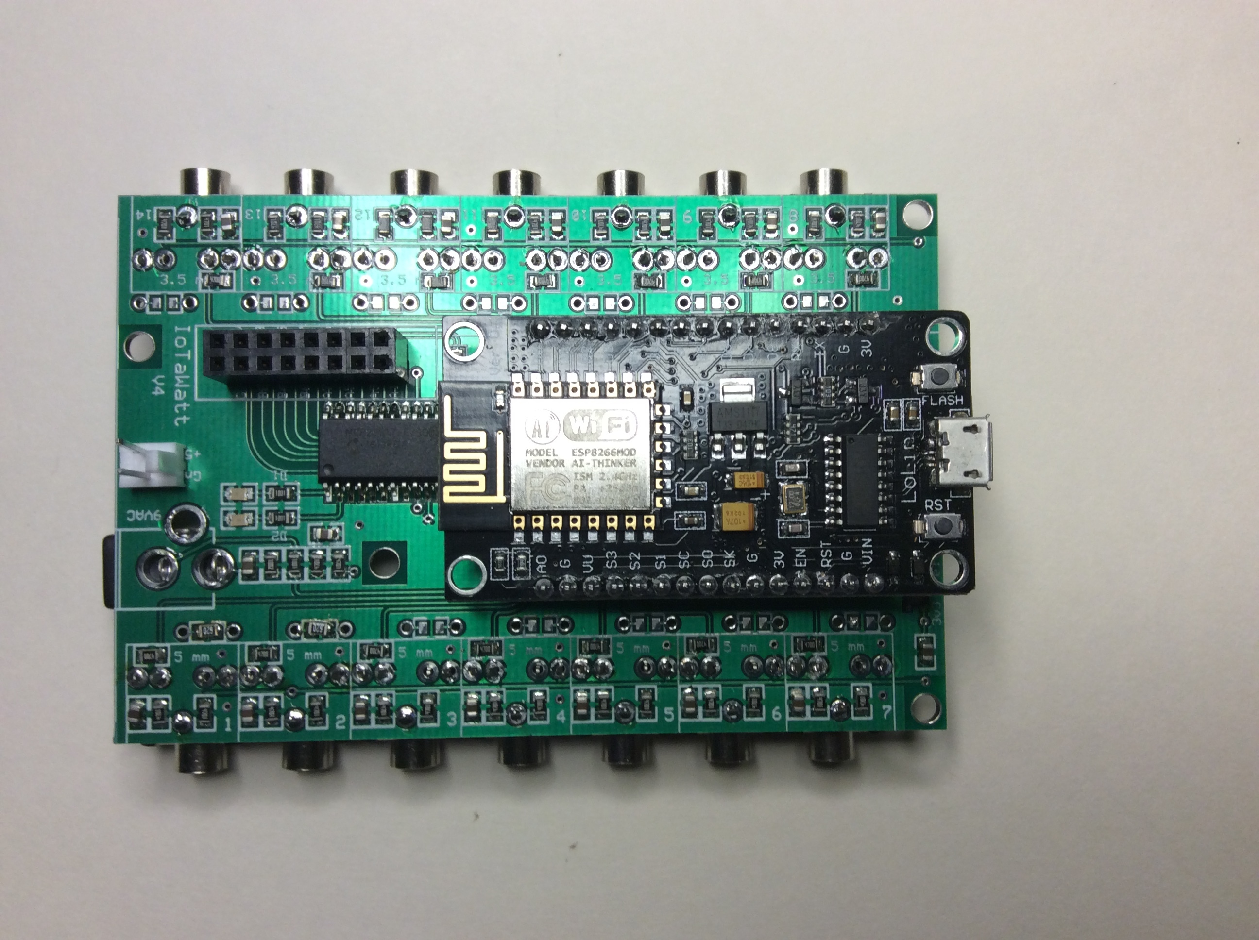
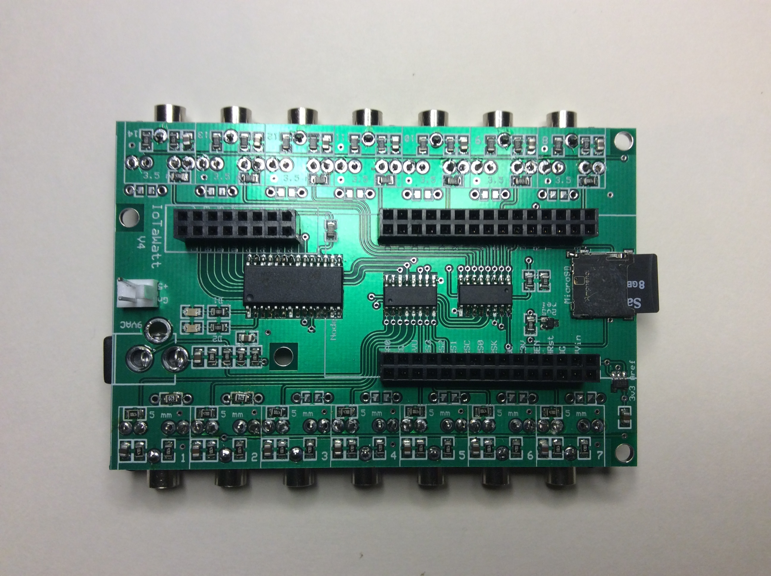
The SDcard is working well. Now the device configuration including the cloud server info and CT configuration is kept in a Json file on the SDcard. The server info including type (emonCMS for now), URL, and apiKEY are kept there, as well as the reporting frequency etc.
Will be storing the feed data and derivatives on the SDcard in the near future.
The big piece left to do is to build an AJAX application to view and modify the configuration file.
Accuracy has been the push in the last few weeks. Built a test rig that is driven by the device itself (reason for the GPIO chip). It provides an accurate calibration factor for a CT. Using a 6V AC power supply, a bank of resistors, and a set of current multiplier loops, the thing subjects a CT to up to 225 different current values from 500ma to 75A and records the CT output. Here’s the output for an YHDC SCT013-050:
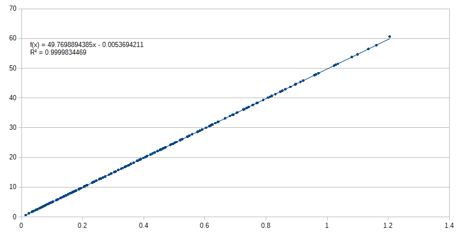
The trend line regression yields the Amps per Volt that should be used to calibrate the CT. (49.7698…or 49.8). As you can see, linearity is good throughout its range.
I’ve tested several of each that I have, including some larger mains type CTs. I’ve got a few smaller doughnut CTs coming in that I should be able to add to the Json database for easy configuration.
Hello @overeasy. Can you share Eagle files of your board?
I’ve posted latest schematic and PCB layout files on GITHUB (search IoTaWatt). They are not Eagle files. They are produced by ExpressPCB’s sofware which is free but as far as I know proprietary to them. I use them because the app seems more intuitive than Eagle and their protopro service (3 boards, $61US, 2 days) works well for me.
Express PCB seems to have a service to convert to Gerber format. See this post.
You’ll probably find that the the phase error introduced by the CT across the dynamic range is a lot less well behaved than any amplitude error.