Checking the HAL drivers seems 1mV accuracy is possible with trimming, whereas to eliminate the jitter between two adc values on our Vref of 2.048V, I’d need 0.5mV trimming accuracy. I think that makes sense…
What range of values do you see without trimming? That’ll tell you the peak-to-peak noise in ADC units.
The range is 3. For example, it is mostly on 2048 or 2049, with occasional blips of 2047.
That’s pretty impressive. That’s with a closed CT wrapped around nothing, connected? Does it go up when you measure big loads with all the other CTs at the same time?
I don’t think so.
The ADC was running…
Only an ac-ac was connected.
I wonder if there are CTs back in stock now. I had only the one to test with before.
The RealPower check before had CT1 connected to an old 100A CT I found with the grey lead. Not an obvious sign of noise during that test.
I could check again with 9CT connected when back on this.
Hello,
New revision here. v1.0
The range on the amps readings buffer with 9 CTs connected is 6.
temp.csv (277.0 KB)
Here’s a piece of the serial output:
--- Miniterm on /dev/ttyUSB0  115200,8,N,1 ---
--- Quit: Ctrl+C | Menu: Ctrl+T | Help: Ctrl+T followed by Ctrl+H ---


Start, connect VT.
Number of boots:17
Reset Cause:EXTERNAL_RESET_PIN_RESET
rPi not connected.
RFM69 not connected.
SPI4 DeInit'd.
ADC DMA buffs: 18000 bytes

{STM:1.0,
V1:247.31,I1:0.099,AP1:24.5,RP1:-0.0,PF1:-0.000584,Joules1:-0.071,Clip1:0,cycles1:228,samples1:47054,
V2:247.30,I2:0.117,AP2:28.8,RP2:-0.1,PF2:-0.001750,Joules2:-0.252,Clip2:0,cycles2:228,samples2:47055,
V3:247.30,I3:0.091,AP3:22.5,RP3:0.0,PF3:0.000661,Joules3:0.074,Clip3:0,cycles3:228,samples3:47055,
V4:247.30,I4:0.091,AP4:22.6,RP4:0.1,PF4:0.002861,Joules4:0.323,Clip4:0,cycles4:228,samples4:47055,
V5:247.31,I5:0.116,AP5:28.7,RP5:-0.1,PF5:-0.002482,Joules5:-0.356,Clip5:0,cycles5:228,samples5:47054,
V6:247.31,I6:0.090,AP6:22.2,RP6:-0.1,PF6:-0.002826,Joules6:-0.313,Clip6:0,cycles6:228,samples6:47054,
V7:247.31,I7:0.091,AP7:22.5,RP7:-0.0,PF7:-0.000662,Joules7:-0.075,Clip7:0,cycles7:228,samples7:47054,
V8:247.31,I8:0.090,AP8:22.2,RP8:0.1,PF8:0.002643,Joules8:0.293,Clip8:0,cycles8:228,samples8:47054,
V9:247.31,I9:0.112,AP9:27.6,RP9:-0.1,PF9:-0.003439,Joules9:-0.475,Clip9:0,cycles9:228,samples9:47054,
Hz:50.0,millis:6001,PC:0,buffOverrun:0}
{STM:1.0,
V1:247.32,I1:0.096,AP1:23.7,RP1:0.0,PF1:0.001664,Joules1:0.126,Clip1:0,cycles1:252,samples1:52001,
V2:247.32,I2:0.115,AP2:28.4,RP2:0.2,PF2:0.005632,Joules2:0.548,Clip2:0,cycles2:252,samples2:52001,
V3:247.32,I3:0.090,AP3:22.2,RP3:-0.0,PF3:-0.001911,Joules3:-0.138,Clip3:0,cycles3:252,samples3:52001,
V4:247.32,I4:0.090,AP4:22.3,RP4:0.1,PF4:0.006427,Joules4:1.039,Clip4:0,cycles4:252,samples4:52001,
V5:247.32,I5:0.116,AP5:28.6,RP5:0.2,PF5:0.007764,Joules5:0.756,Clip5:0,cycles5:252,samples5:52002,
V6:247.32,I6:0.091,AP6:22.5,RP6:-0.0,PF6:-0.001849,Joules6:-0.522,Clip6:0,cycles6:252,samples6:52002,
V7:247.32,I7:0.093,AP7:23.0,RP7:0.2,PF7:0.006632,Joules7:0.689,Clip7:0,cycles7:252,samples7:52002,
V8:247.32,I8:0.091,AP8:22.4,RP8:0.0,PF8:0.001497,Joules8:0.461,Clip8:0,cycles8:252,samples8:52002,
V9:247.32,I9:0.109,AP9:26.9,RP9:0.1,PF9:0.004691,Joules9:0.156,Clip9:0,cycles9:252,samples9:52001,
Hz:50.0,millis:11045,PC:0,buffOverrun:0}

Cheers
Nice! So 6 ADC units represents 117mA?
What happens if you put max deflection through Chs 1 through 4 and 6 through 9. Does Ch5 stay at 116mA?
We have different reference and burden values now so 6 units would be 2.048V / 4096 * 6 = 3.5mV…
3.5mV / 6R8 = 0.51mA
I swapped the burdens for 150R to amplify the signal and did the test you’ve recommended and it’s interesting.
{STM:1.0,
V1:243.35,I1:192.842,AP1:46928.8,RP1:46718.5,PF1:0.995518,Joules1:582116.627,Clip1:0,cycles1:250,samples1:51491,
V2:243.35,I2:193.429,AP2:47071.3,RP2:46903.1,PF2:0.996426,Joules2:587440.909,Clip2:0,cycles2:250,samples2:51491,
V3:243.35,I3:192.359,AP3:46811.0,RP3:46546.8,PF3:0.994357,Joules3:591039.921,Clip3:0,cycles3:250,samples3:51491,
V4:243.35,I4:194.997,AP4:47453.2,RP4:47309.3,PF4:0.996968,Joules4:604604.068,Clip4:0,cycles4:250,samples4:51491,
V5:243.35,I5:0.138,AP5:33.6,RP5:22.4,PF5:0.667002,Joules5:305.595,Clip5:0,cycles5:250,samples5:51491,
V6:243.35,I6:193.072,AP6:46984.7,RP6:46816.3,PF6:0.996415,Joules6:602616.160,Clip6:0,cycles6:250,samples6:51491,
V7:243.35,I7:191.942,AP7:46709.2,RP7:46508.9,PF7:0.995712,Joules7:603558.030,Clip7:0,cycles7:250,samples7:51492,
V8:243.35,I8:193.096,AP8:46990.1,RP8:46832.3,PF8:0.996643,Joules8:636185.917,Clip8:0,cycles8:250,samples8:51492,
V9:243.35,I9:193.876,AP9:47180.2,RP9:47007.8,PF9:0.996347,Joules9:632255.640,Clip9:0,cycles9:250,samples9:51491,
Hz:50.1,millis:86025,PC:0,buffOverrun:0}
There’s a small effect on the remaining channel.
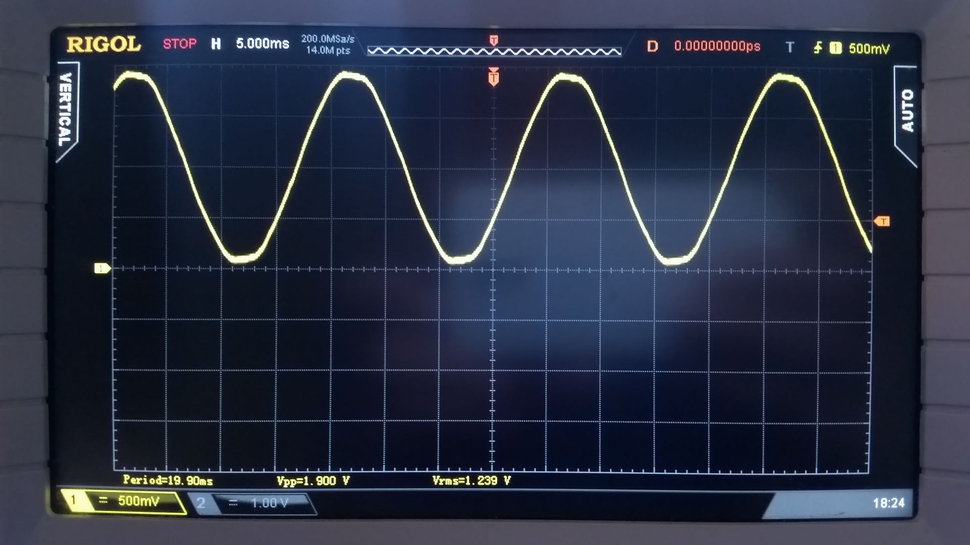
This a trace of the signal:
and this is one on the remaining channel:
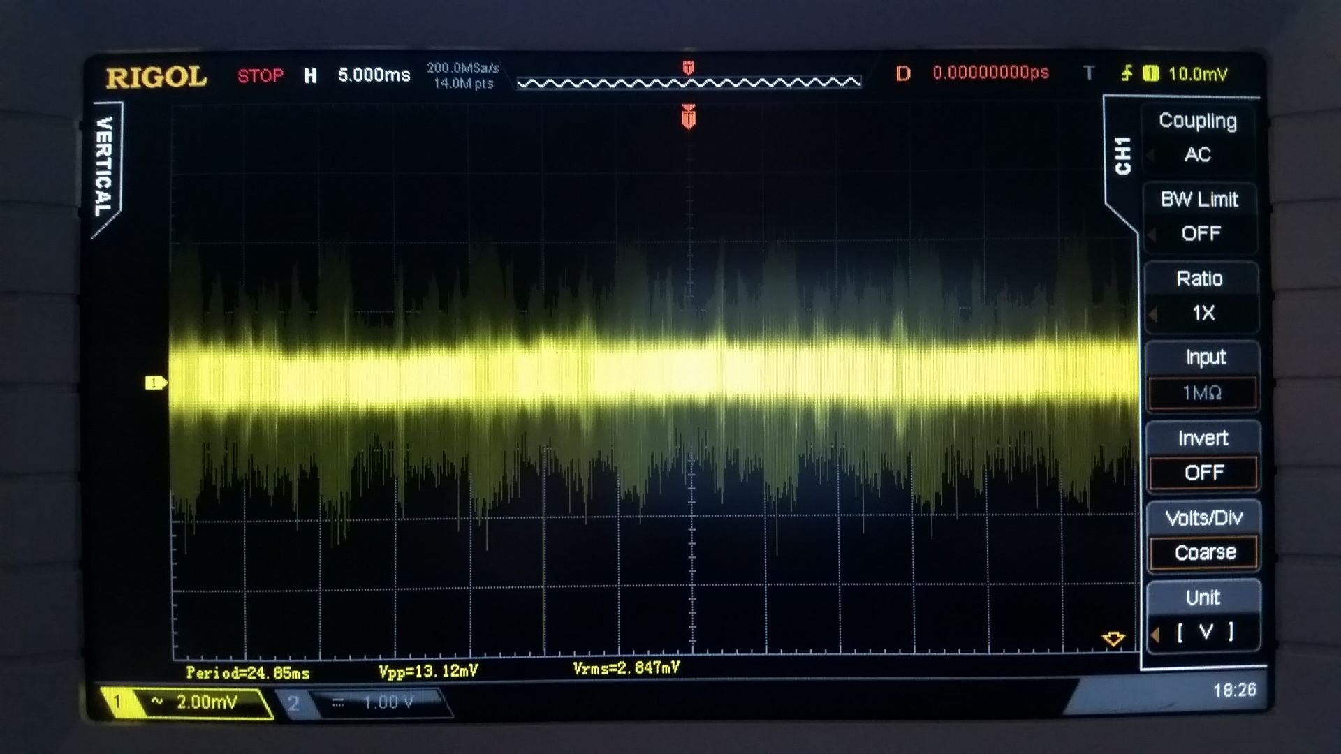
I see a slight wobble and a ton of noise. The load is a fan heater on half-power. I have those nicer loads to test with so I’ll have to bring them in to the lab some time.
On the plus side, the signal is represented by a notional current reading of 193.072, against the wobbled channel at 0.138, so there’s a ratio there of near 1400 anyway. Considering how noisy the signal is, not bad. Also, the background noise doesn’t look too bad with this scaling. Also, comparing 0.138 against the 0.101 below says something.
This is the standby with no load:
{STM:1.0,
V1:248.47,I1:0.566,AP1:140.7,RP1:73.2,PF1:0.520446,Joules1:1459.198,Clip1:0,cycles1:250,samples1:51590,
V2:248.47,I2:0.567,AP2:141.0,RP2:72.9,PF2:0.517241,Joules2:1454.899,Clip2:0,cycles2:250,samples2:51590,
V3:248.47,I3:0.565,AP3:140.4,RP3:73.9,PF3:0.526785,Joules3:1471.969,Clip3:0,cycles3:250,samples3:51590,
V4:248.47,I4:0.571,AP4:141.9,RP4:72.7,PF4:0.512003,Joules4:1446.058,Clip4:0,cycles4:250,samples4:51590,
V5:248.47,I5:0.101,AP5:25.1,RP5:-0.2,PF5:-0.007526,Joules5:-2.065,Clip5:0,cycles5:250,samples5:51591,
V6:248.47,I6:0.566,AP6:140.7,RP6:72.0,PF6:0.511382,Joules6:1429.917,Clip6:0,cycles6:250,samples6:51591,
V7:248.47,I7:0.563,AP7:139.9,RP7:72.1,PF7:0.515435,Joules7:1434.946,Clip7:0,cycles7:250,samples7:51591,
V8:248.47,I8:0.566,AP8:140.6,RP8:71.9,PF8:0.511241,Joules8:1432.945,Clip8:0,cycles8:250,samples8:51591,
V9:248.47,I9:0.570,AP9:141.7,RP9:73.3,PF9:0.517334,Joules9:1461.866,Clip9:0,cycles9:250,samples9:51591,
Hz:50.0,millis:21036,PC:0,buffOverrun:0}
Shall I get the buffer readout direct for ya? Seems the noise will make it appear gobbledigook anyway, but I could try with the more linear loads tomorrow if you reckon?
@dBC p.s. Seems some of that noise was gnd noise. I’ll dig in a bit deeper…
I figured out a way to print out the single channel buffer values.
The range on ch5 with all other channels with a 1.6V peak-peak signal on them is 22.
A fair bit up from 6.
| no ct | with ct | no ct + load on | with ct + load on | |||
|---|---|---|---|---|---|---|
| 3 | 6 | 22 | 22 |
ch5.ods (23.3 KB)
A relevant paper on capacitors under DC bias.
capacitance-change-vs-voltage-ceramic-capacitors-1.pdf (446.5 KB)
I’m a bit of a latecomer to this topic. I read through the entire post yesterday and it very much sparked my interest, but disappointed that it appeared to have stalled. my interest is in 3ph usage.
However @TrystanLea confirmed in another topic that work will restart this year.
I’d like to make a few observations on what I’ve read in this topic:
- I’d give a thumbs up to the proposed green connectors. The company I work for uses those connectors quite broadly, the are very reliable. We have products in the field nearing 15 year old.
They make test, service and debug very easy and even non-technical customers can easily board swap in the field.
-
ESD diodes, I think this has been mentioned by other contributors, we widely use BAV99L for ESD protection. It has both diodes in a small SOT23 pack and widely available.
-
Voltage reference, we use the ADR5054B of all our ADC references. It’s a 2.048v ±0.1% diode reference in an SOT23 package, there are different voltages available
When I looked at the v0.9b schematics, I saw the 3ph voltage input was 3 x 3.3v AC input, whereas the 1ph was still 9v. I could find no mention as to why this is or what will be used to generate these small AC inputs. Can anyone enlighten me on the thinking behind that decision?
I look forward to the restart.
Chris
Hi Chris,
Here’s the prototype 3-phase unit, DIN rail mountable, for connecting to the new stm32 unit. It’s based on ZMPT101B ‘voltage sensing transformers’, which are actually CTs themselves.
https://github.com/danbates2/ZMPT101B-3_Phase-DIN
I believe an outstanding aspect of the design to confirm was making sure the live-side resistors were suitably spec’d for a worst case scenario, including damp environments.
I don’t know the relative states of the repos but my own working one was this: http://github.com/danbates2/stm32
Thanks for the update
This link appears to be broken, I did also check out your root github doesn’t seem to be listed there. I do like the idea of the sealed sensor. At work we use Vigortronix sealed transformers.
Thanks, I’ll take a look.
Chris
The repo was private, it’s now public. Please try again.
I’ve given myself a reminder, when I’m next at a proper computer, to include some safety related notices on the 3phase sensor’s github page when I next can.
Thanks for taking a detailed look at the project.
Daniel, Thanks.
I suppose I’m quite lucky as at work I test 3 phase kit, so have a healthy respect!!.
At home I’m currently using the Robin Emley 3 phase PCB.
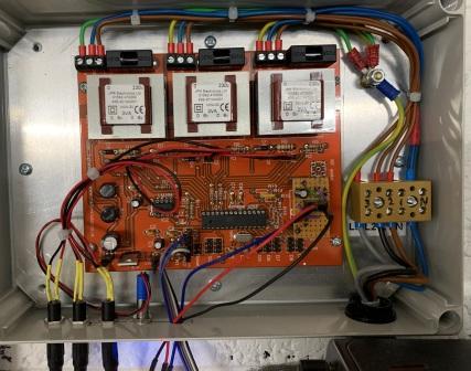
For my connections I have a 3pole linked MCB in the fuse box, the lowest current I could get was 6amp, then a 4pole isolator, which is then wired to the PCB with 100ma fuses.
Sorry for the 90 degree rotation I can’t make it the right way up!
I’d much prefer to to have low voltages coming out of the fuse box.
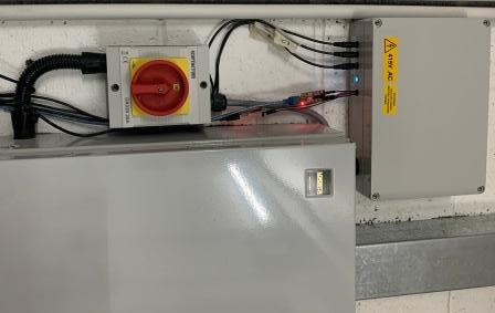
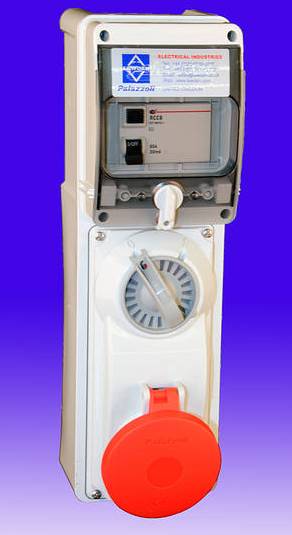
At work I have a combination 3 phase outlet for connecting to kit I’m testing.
Chris
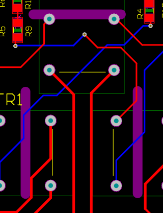
You might want to review that layout to make sure you’ve got a clear continuous 8mm isolation strip on the PCB between the primary side and the secondary side. You may already have it, and it’s just unclear from the photos, but with that offset and rotated transformer, it looks like it could be tricky to achieve.
I think there’s something like that despite the zig-zagging isolation line… needs checking. Where does the 8mm come from?
Safety standards like IEC-60950 (now replaced by IEC 62368-1) and IEC 61010 require reinforced insulation between primary circuits and SELV (low voltage safe) secondary circuits. To accomplish this they call out specific creepage and clearance requirements between the two areas. In addition any component that straddles the reinforced insulation boundary must meet the particular safety specs. The PCB creepage and clearance distances are determined by the working voltage of the circuit and also the over-voltage category which is related to where in the electrical supply it is situated. The over-voltage category determines what surge voltage the reinforced barrier must be able to withstand. For most circuits with a working voltage of less than 300V the creepage distance is between 6.4 and 8mm. Additionally, as the transformer straddles the safety barrier it must also meet reinforced insulation requirements and should have a UL, TUV or similar safety approval to be used in a product.
Daniel, I took a look at your v0.3 eagle files, looks like you have a mil slot defined, but it didn’t come through well when I opened the files in Eagle V9.6.2 and some tracks were crossing the mil slot. Maybe it’s a version thing.
I imported the PCB into Altium and got this:
I haven’t looked at your previous versions yet.
I notice the two bottom two transformers were 90 degrees to the top one, is there a reason? space in the case? It makes the isolation a bit more complicated.
I’ve ordered a few of the ZMPT101B modules to have a play with.