What amount of load are we talking about? Say for our typical AC adaptor?
How do you envisage that working with regards getting to the three V signals? Some sort of electrician installed DIN-rail mounting?
I’ve never checked that, because I know it would be a non-starter.
Sounds like we’re in the 1.21 Jigawatts ballpark 
I don’t have enough experience to suggest a solid and feasible idea.
The only idea which attracts my crazy inventor-self I wouldn’t dare suggest so late on a Tuesday night.
I think a sensible unit would be a voltage-sensing-transformer based unit. And I believe 4 connections would be necessary on the dangerous-side. The three phases and Neutral. Downstream, three cables would be coming from the output of this box 2.1mm plugs and jacks for simplicity’s sake, the cables terminate at the barrel jacks plugged into the stm32Tx unit we’re working on. These DIP switches would be switched in to bypass the 120k input impedance…
DIN rail mounted, sure why not.
edit: @dBC
I was mostly interested in how you do away with “not having to install 3 separate sockets”. I guess you install a 3-phase socket, or you whack it on the main DIN rail where you can get access to all 3 Vs.
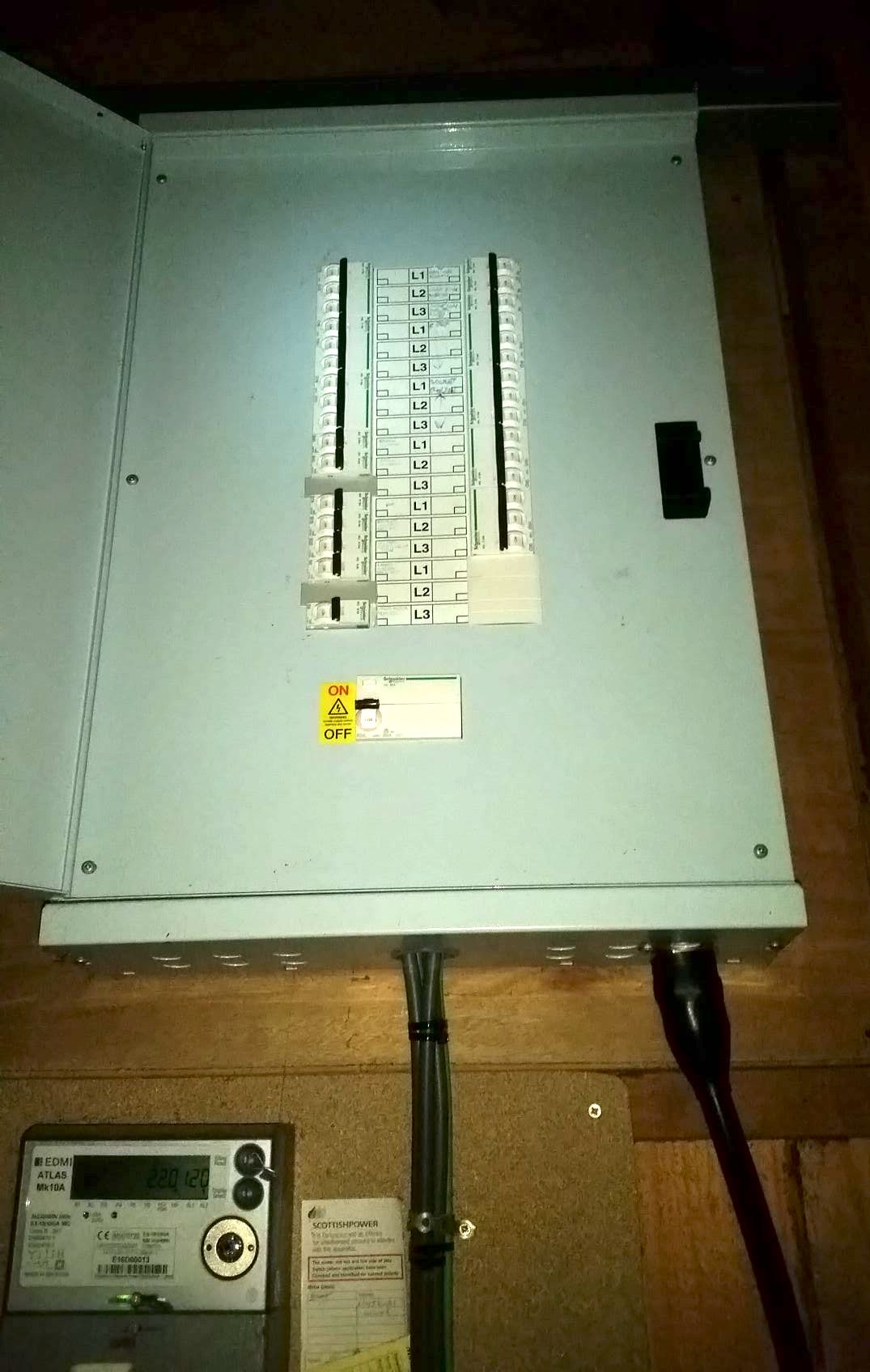
Inside the consumer unit?
I really don’t have enough experience, Glyn would have some good ideas on this I bet.
What’s a 3-phase one of those? I don’t think one exists - you’d almost certainly be looking at a “small industrial” distribution board for 3-phase; or for domestic, I think 3 separate consumer units would be much more likely.
And then, if you have one consumer unit per phase, how do you have a 3-phase socket connected to those, because you need a linked circuit breaker for safety and to prevent single-phasing should a motor be connected. It gets very messy.
I believe you.
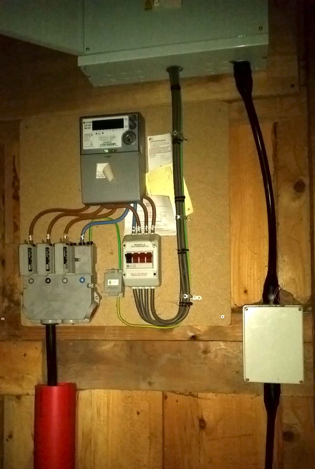
Hmm. There’s a 3-phase distribution board in one of the sheds here where I live. It serves the wood workshop machinery. I’ll have a look inside tomorrow. Poke around (not really).
Still alive.
I think it’s my common sense telling me, something like “don’t bloody touch anything”.
The question of what physical unit @dbc could be conceived to monitor voltage and current at a set up like this, I’m still not sure.
I guess one way of doing it could be to have a unit with…
. A strong enclosure with anti-tamper top.
. Chunky screw terminals for 25mm meter tails.
. Battery power, a year’s worth a data guaranteed, radio transmitted to an emonBase or stored locally.
That’s for something mounted in-line with the cables after the main breakers. Basically a matter of designing a 3-phase meter.
Beyond that, inside the large metal dist. board I imagine the DIN rail possibilities mentioned.
@danbates & @TrystanLea very nice work!
Dan, I fell upon your recent v1.0 on Github. I noticed there’s a lot of protection diodes (36?), which is definitely a good idea. You may want to consider using something like this to cut down on that D list: https://www.mouser.com/datasheet/2/308/ESD1014-D-1805060.pdf
Looks good. Thanks!
I had a closer look at the diode situation recently actually. Did you notice the pair of larger schottky’s on the bias? It crossed my mind those could do the job of the 20 input diodes, 18 on the ct’s plus the 2 on the ac-ac input… because of the nature of the circuit… low burden resistance and the 9k1 on the LPFs… Tricky one that 
The latest board (v0.9) performs well enough in many ways.
Sitting on a bench, with an ac-ac connected, the real power readings across channels is consistently below a Watt.
Averaging over a minute it was ±47mW across channels.
serial output.ods (26.0 KB)
As a representative of noise it’s an improvement on the last version.
More news coming soon…
Ah, you’re right, I didn’t even think about combining all of those. That makes a lot more sense. I see how careful everything was laid out with them, and ferrite beads - I assume those are also to correct for noise?
I was going to ask about the bias. Is it just to control for gain on the CT and VT inputs depending on the voltage reference?
Yeah, the ferrites were mostly there for testing. Some will be 0R, some may be found to be useful… I’ve recently got hold of a book of 0603 ferrites and am going to make sure the most noisy USB adaptor I can find doth not even disturb the readings too much.
The bias is a midrail from vref. All adc readings are converted as a ratio of analog ground to vref, so the opamp bias should be in the middle somewhere, supplying all the ct’s and ac-ac adaptor with a midrail. So it’s not for controlling the gain of the inputs, it’s just a mid reference for the AC signal.
Bit more in depth…
That v1.0 does have a new method of getting the midrail… Scaling down the vref by 10, and then back up with a gain of 5, so it ends up in the middle. Risk is it’d scale up noise also, but it’s meant to work in conjunction with the feedback capacitor (compensated opamp) so high freq noise has a gain of near 0, so helping with a stable bias. I’m not convinced of this myself yet, and might go back to a simple 10/10k divider and follower. After I tested v0.9 and even trying a couple different opamps, I came to think there may ultimately be noise coming from the opamp, and may be 100% inherent and unavoidable.
Not trying to knock your achievements here, but I find Irms is much better than RealPower when trying to get a handle on how much noise you have. That dot product with V is an almost perfect filter - removing everything except for the 50Hz content (to the extent that your V signal is a perfect 50 Hz sinewave). So a RealPower of 0W really just says you’ve eliminated the 50Hz noise in the I signal. An Irms reading of 0 says you’ve eliminated all noise in the I signal. That’s important if you want to accurately measure ApparentPower and PowerFactor.
True. That’s what we were doing before, comparing v0.8 to v0.9 the Irms noise is improved. I’ll make a table and show the improvement version to version…
@dBC the transistor method gave a usable and fine bias, but the best Irms result was with the 1k 1uF snubber with a compensating feedback loop. Wishing I took pictures and saved numbers but I just stormed through the tests instead as I want to get this project done. Forgive me! There was a roughly 20% difference between having the transistor there or not. The gain of the tranny must make it tricky to control tightly. Thinking that opamp-tranny combo would be ideal for a mosfet driver, dealing with that capacitive gate?
The next revision has the ref191 Vref coming off the Analog3v3. Now that it’s 2.048V it can be powered from 3v3 instead and decoupled easily from the noisy 5V. Might even achieve something better yet again.
The icing on the cake might be to make use of opamp trimming. It’s a feature I noticed of the stm32 opamp. Have you used it yourself? My thinking is to trim the output to steer the opamp away from an output near the boundary of two adc values, so the ADC reads a more settled 2048. I can think about these things while waiting on other things and taking a break.
Apart from this rudimentary experiment for you guys a few years back, I’ve not used stm’s internal op-amps at all. Processor pins are a limiting constraint on most of my projects, so I don’t want to waste any on h/w that can so easily be added externally.
Cheers. That’s interesting as an approach, to go for an MCU with a lower pin count and then use more external ICs. I guess this is for the purposes of value engineering? We know here the stm32’s with the higher pin count are a fair jump in price.