STM32 Hardware Development

Thanks @daturach for the tip, I have now found and downloaded the stm32cubef3 examples. I can see a couple of Opamp examples but not for the STM32F303RE. I have now tried various combinations of positioning the HAL_OPAMP_Start() following one of the examples for other variants but still no luck :slight_smile: does the opamp depend on any other features such as the DAC or a timer setting or something like that?

Just a SWAG, but is any of this relevant?
From Reference Manual (RM0316) Pg 470.

Have you tried PA6/PA7 since introducing the calls to HAL_OPAMP_Start()?

What state are your SB62 and SB63 jumpers in? The default is open, which means D0 and D1 on the Arduino headers won’t be connected to anything.

When I’m starting a fresh project using a Nucleo board (as opposed to using a virgin chip on my own board) I always use the “Board Selector” in the GUI and then when prompted “Initialize all peripherals with their default Mode?” I always select Yes. That way any pins that are in use by the board will be flagged as in use. Even if I don’t plan using the UART, the LED or the Button, those pins are wired through to those features on this board, so having them flagged as in-use reminds me to stay away from them and use a Grey pin instead. If I absolutely have to use those pins for my feature instead of their feature, then I dust off the board schematic and work out what jumpers I need to change so as to disconnect their feature, and connect mine.

If you start with a virgin STM32F303RETx board in the GUI, you get this:

An example of that is using the second channel of the DAC. It can only be output on PA5 which is hardwired to the Green LED. That LED puts a big enough load on the signal that it can’t drive it all the way to 3.3V (even with the buffer enabled), so on the Nucleo board that I use for DAC testing I’ve had to remove SB21 and I can no longer use their LED.

Don’t underestimate the value of being able to do console printfs when the debugging gets tough. That’s saved my bacon lots of times. LEDs and GPIO toggles are great for timing stuff but there are times when you really need to see the contents of a 32-bit h/w register to find out what’s really going on.

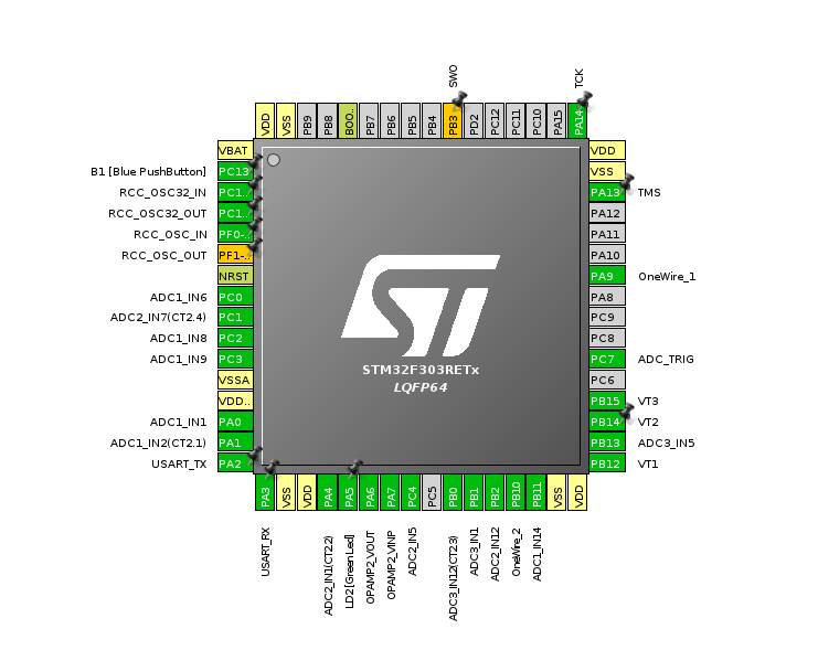
So I pinched PA6 and PA7 from the CT input scan on the emonTxShield demo (they weren’t being driven anyway) and used them for OPAMP2 in follower mode. So my pinout now looks like:

Then I hooked up the signal generator to PA7 with a rail-to-rail triangle signal (Yellow trace) and also probed the output PA6 (Green trace). The datasheet says the opamps are good for 0.5 mA so I loaded up PA6 with a 6k R to GND. The Pink trace is Green minus Yellow (i…e. output - input).

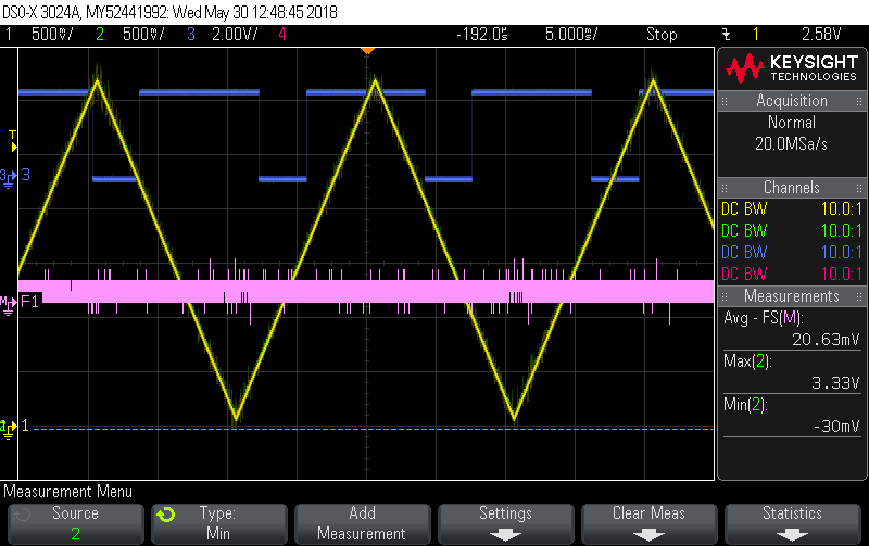
The results are pretty good. Green is so identical to Yellow you can’t really see it. Pink shows about a 20mV offset between the two. I tried with the factory trimming and the user trimming but I couldn’t notice any difference to the ~20mV offset. BTW, if you do want to do a user trimming and self calibration, you can do all of that from the GUI under Configuration->OPAMP2. It’ll then generate the call to HAL_OPAMP_SelfCalibrate() for you, from within MX_OPAMP2_Init(), after it’s called HAL_OPAMP_Init().

[EDIT] - actually I see the exact same 20mV even when I connect both probes to PA6 so I think it’s just a scope measuring limitation rather than an indication of an offset out of the opamp.

Fantastic, Opamp2 on PA6/PA7 works!! :slight_smile: I’ve got a 10uF capacitor across my 470k:470k voltage divider, with an LED on the output you can see brightness change as I switch the top resistor to 150k, great!

1 Like

Yes they are both open, thanks for the tip, much appreciated!

I neatened up my USB DFU (right) and Opamp testing (left) circuits this morning, ordered a USB mini adapter rather than having flying leads on the end of a USB socket with the risk of shorting the connections. Still same error on USB, I still need to look into the BOOT1 bit question.

Ken Boak introduced me to small energy monitoring development board with a supercap and FRAM on it a while back. I’ve done a quick calc to see if the RTC can be powered from a supercap instead of a coincell, which would be good in principal.

Typical current draw at VBAT is 0.5uA, 1uA max., according to STM guide.
I’m assuming the RTC uses the internal high speed clock and assuming the guide’s figure is based on using the internal clock.

The leakage current of this 1F cap is about 2.1uA, worked out from the discharge over time graph, 100h charge time.

http://mustcalculate.com/electronics/capacitorchargeanddischarge.php?vfrom=3.3&vto=1.65&vs=0&c=3&r=1269230.7692

“Resistance” at above site worked out as 3.3V / 0.0000031A.

614 hours or 25 days.

With a 50% drop in performance, seems usable for most contexts…

EDIT: I guess my main question on supercap vs battery is whether or not the time will be set during programming before shipping, would a short shelf life for an RTC be an issue for the OEM crew? Or does the module get time from an ESP or other internet connected MCU?

Doing a bit of a review of my local CVS respository, I noticed I had outstanding changes on the emontxshield project that related to enabling the opamp as described above. I figure that’s probably worth capturing the in the tar file series (and @pb66’s github repository) just to show how it’s done. While I was there I also included the opamp output in the ADC scan so have included that as well. The plot below is graphical representation of the DUMPING output you get if you dump that “channel”, you can see it matches the scope traces of the triangle wave above and has no trouble going rail-to-rail.

I’ll post a new version of the tarfile in the main thread to keep them all together.

Thanks @dBC for the advice on adding the RX and TX lines to the ST-LINK connector in the PM, thought I would move the discussion here for everyone’s benefit, is there a recommended standard pin order/connector for ST-Link with rx/tx lines?

Im wondering if something like this would work, a combined UART & ST-Link 8 pin header. First 6 pins would program using one of our standard UART to USB adapters, SWDIO and SWCLK added on top to provide ST-Link option:

Here are a few photos of our new dev board.


below: with solder paste.

a beautiful 100-pin stm32f303


Notes on design to follow in a separate post.

Trys and I are keen to develop the smaller board in parallel. 1VT and 3CT sat on top of an rPi. Something we need to cost out. I think there’s a post somewhere showing this?
Yes: STM32 Development - #280 by TrystanLea

1 Like

Wow! You guys have been busy. Well done! I gotta’ ask… what does CLMP stand for?

1 Like

CLAMP!
I like the look and feel of these:
. 1822765 Phoenix Contact | Mouser United Kingdom

P.S. Thank you :slight_smile:

Despite having a poor camera on my phone I had to share. Got Blink working on the virgin chip!

It involved using ST-Util on Windows :scream:

Is there an alternative?

1 Like

Fantastic progress @danbates! :slight_smile:

Could you upload using method documented here?:
STM32/Blink.md at master · openenergymonitor/STM32 · GitHub

Yes, once the first flash is made the copy-to-volume method we’ve used before works fine.

I’ve added a note on the readme and a doco page.
. https://github.com/danbates2/STM32/tree/db#hardware

Doh! I’ve got Tx and Rx on UART2 swapped, so the FTDI header is out of action.

UART1 debug out is working fine.

Got it!

08

RST pin needs the 100nF cap, I had to bend it out of the way for the chip to run.

Pics of the rPi ontop here…

Some details not easily seen in the photographs:

  • CT and VT ADC inputs routed to allow synchronous sampling. (4 ADCs available on our chip) Expansion module 6 CTs planned should also be fine with synchronous sampling.
  • RJ45 connector included following combined pinout for optical sensor and temperature sensor compat.
  • Lots of solder jumpers placed to play with either SPI or UART data transfer between the rPi, STM32, and ESP8266 module.
  • DIP switches on CTs 1,2 and 3 to switch out burden resistor.

A few notes from convos with Trys:

  • We’re looking for an all rounder 3-phase native board with rPi mount, which doesn’t cost the earth.
  • Case design as custom injection molded case. Clean, simple, white, rounded corners. Screwless with a pop-off inset lid ideally.
  • Replacing the esp8266 based module with an esp32. Without rPi, this gives great standalone features.
  • USB-C will be the power-input connector.
  • clamp connectors to be versatile, a mix of I/O and analog. Expansion module has similar thinking around it, with provision for at least 6 more CTs, do we need extra VTs?

A few notes of my own:

  • USB DFU enabled chip seems possible. CubeMX auto clock config has shown it’s possible… so far not got it work. Anyone here with experience in this?
  • microSD and supercapacitor footprints, for local logging of large volumes of data, and maintenance of the RTC in case of power-outage.
  • Undecided on best way to route the wire-clamps, at the moment each triplet has 5v pwr, 5v tolerant in/ 3.3V out, and gnd. Could be nice to go for a triplets of: 5V 5V 5V. 3V3 3V3 3V3. Signal Signal Signal. Signal Signal Signal. GND GND GND.

Many thanks.

2 Likes