STM32 Hardware Development

Should be just:

sudo service emonhub status

and:

sudo service emonhub stop

:slight_smile:

1 Like

Got it, UART1 catching data from rPi, transmitting then on UART2.

11

Seems like these more basic HAL functions are useful for fixed data-lengths.
DMA or Interrupt modes are going to be better for us to use I think, for varying data lengths.

RFM69CW testing:

I’ve got an rPi talking to an RFM69. Basics from here.
https://rpi-rfm69.readthedocs.io/en/latest/hookup.html#wiring
The python wrapper is based around the (much better) LowPowerLab library.

I’m changing our stm32 board to match this guide. Or… do I change it to match the existing emonPi pinout?

Confirming the pinout…
The emonPi is making use of the ATMEGA for sending data thorugh the radio module.
Trys and Glyn I think want to have the rPi doing the comms management, it’s better.

I’ll include solder jumpers to connect the stm32 to the rfm69. The default then will be rPi/ESP connected to the rfm69. We do already have an stm32 functioning with rfm69 documented, so including the code as an option, without ESP or rPi, exists.

Cheers.

P.S. I had to do this outside of our stm32 board, because I had different routing from the rPi library here. Although there’s a way to override pinouts, I tried it and I couldn’t get it working.
Hence changing the routing for the next revision :slight_smile:

Scroll down for board-revision update.

A prototype 3D printed enclosure here. I received lots of advice on injection moulding yesterday from the manager of our local fabLab.

It’s a lasercut piece of acrylic ontop.

SPI testing

I’ve got some outputs with SPI this morning. Following a guide here.

An F103RB Nucleo is sending over SPI as master:

/* Infinite loop */
  /* USER CODE BEGIN WHILE */
  while (1)
  {
    for (;;)
    {
        char message[] = "Hello, World";
        HAL_GPIO_WritePin(GPIOB, GPIO_PIN_6, GPIO_PIN_RESET);
        HAL_SPI_Transmit(&hspi1, (uint8_t *)message, strlen(message), HAL_MAX_DELAY);
        HAL_GPIO_WritePin(GPIOB, GPIO_PIN_6, GPIO_PIN_SET);
        HAL_Delay(10);
        //HAL_GPIO_TogglePin(GPIOA, GPIO_PIN_5);
        //HAL_Delay(1000);
    }
    /* USER CODE END WHILE */

    /* USER CODE BEGIN 3 */
  }
  /* USER CODE END 3 */
}

and an F476 running Analyzer2Go demo.

Wired together:

here’s the Analyzer2Go screen on Windows:

Nice.
So that’s stm32 as master.
I need stm32 as slave.
and run a program on the rPi as master eventually.

Next tutorial: Connecting 2 STM32 boards via SPI – VisualGDB Tutorials


Top Right: Master.
Bottom Right: Slave.
Left: Analyzer2Go.

Getting glitchy comms:


Only single character ‘H’ back and forth works, only some of the time. I’ll be diggin into this another day unless someone has a look at this first?

uploaded to git so far as test2.
. https://github.com/danbates2/STM32/tree/db/Software

For reference: This post and reply has an intro to the idea of using a counter at the stm32 slave, to ensure integrity of the data.

New board revision here:
Checking it over now… could have another prototype on it’s way by end of day.

Had an interesting chat with Glyn about manufacturing / testing processes. Having pogo-pin compatible testing points and a proper testing rig, because, the reality of manufacturing demands we find faulty board quickly!

UART flashing fixed in this version, and a bunch of SPI related changes, and we now have the ESP32 footprint on-board. Going as far as possible with SMT too, instead of through-hole.

Cheers.


(noticing the board outline is very faint, it is there.)

v0.6 stm32-pi.sch (1.4 MB)
v0.6 stm32-pi.brd (524.3 KB)

1 Like

I’ll be keeping major news updates on the other thread and use this thread for any detailed dev.

Cheers

Hi @dBC, happy new year!
Quick few questions here if you’ve got a moment.

When using the timer to trigger the ADCs, does the timer continue to pulse every interval x? and does this effect the functioning of the ADCs continually?

I seem to have a situation where what looks like ADC 1 and 3 are slightly out of sync and I’m trying to get to bottom of it. Possibly it’s because the chip’s been re-flowed a couple of times, it’s had a lot of heat and something could have been put of of whack, hard to say, ordered a new chip just in case.

Connected issue I think: also getting low readings on one of the ADCs, only 80% of what’s expected based on the previous protoboard; 200Vrms instead of 250Vrsm, triple checked all the resistor values, op-amp and the VREF input, which is connected to the 3.3V reference, and I can’t find a fault, another reason to get a new chip… I’ve gone over the code a few times, it’s copy and paste from the working program.
Have you had a similar experience? Here’s the out-of-sync ADC conversions showing up on VREF. I don’t remember seeing this on the previous board.

1 Like

Happy new year to you too!

From memory it was a single pulse with one ADC starting on the falling edge and the other starting on the rising edge. The pulse width is then used to stagger their start times. That was two years ago, so I may be mis-remembering, but there are details here. You’ll see I also plumb the timer output to a spare external pin for scoping/debugging, so you could potentially do that to find out what’s going on. If you want them to start at the same time, you should configure both ADCs to start on the same edge - falling or rising, doesn’t matter.

Multiple pulses? It shouldn’t do. Those edges are just used to start the ADCs running. Once started they run forever and ever and ever… in the spirit of “let no mains cycle go unmeasured”.

If I’m reading your scope trace correctly that’s about 640nsecs between starts, and you’re running the core at 120MHz? That might be the time of two back-to-back calls to HAL_ADC_Start_DMA() - which would suggest they’re set to “triggered by s/w” instead of “triggered by timer edge”. Is the 640nsecs consistent? One way to test that theory would be to put a bit of code between the two calls - nothing substantial (so not a call to HAL_Delay()) but maybe just toggle a spare IO pin 10 times and see if the 640 nsecs grows accordingly. Between that and a scope probe on the timer output, you should be able to work out what’s going on.

Where exactly is that scope probe connected? A 200mV dip on Vref during conversions looks like a big problem to me. While it might be useful for determining when the ADCs start running, once that’s sorted you probably need to make those dips go away if you want accurate readings. You really want Vref to be totally noise free.

Can you run the two boards side by side, fed from the same VT? Then you could probe the two signals at the the ADC inputs and see if one is 25% larger. I just noticed in your schematic above you appear to have the same problem as described here (skip the first paragraph and start at “I wonder if your voltage divider and LPF are working the way you think they’re working”). Your Thevenin equivalent circuit looks something like:

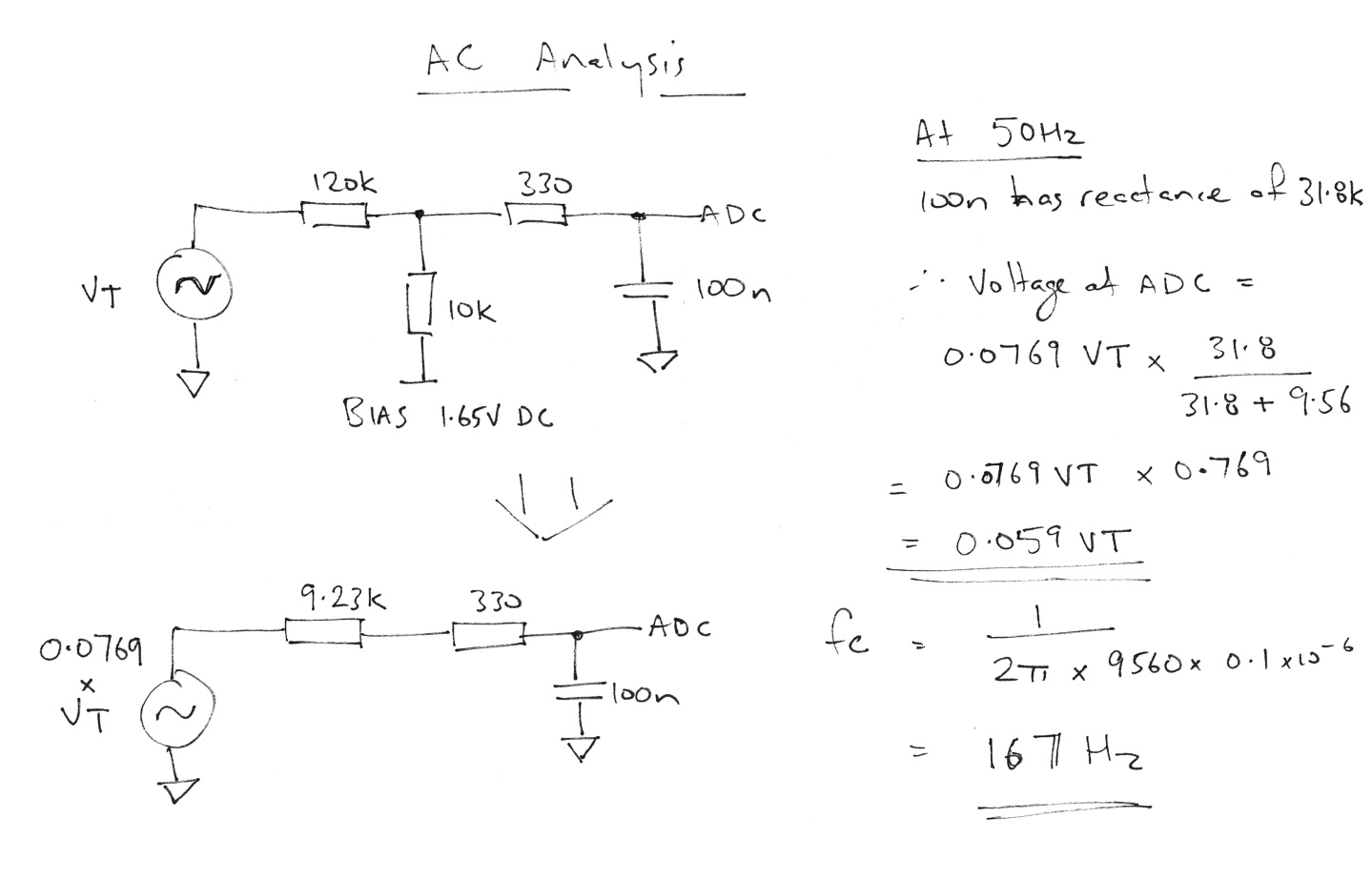
So I suspect your cut-off frequency (167 Hz) is much lower than you were planning, and your divider is reducing the voltage more than you were planning (/17 instead of /13).

P.S. Sorry about the 19 day delay in responding… I only got notified of your post this morning.

P.P.S. That inadvertent savage cutoff frequency also means a massive phase shift of about 16.7°, while the phase shift of the I LPF is closer to about 0.6° so between them, the LPFs have added about a 16° net phase error… or about 0.9 msecs at 50 Hz.

It was yesterday I posted! I had to edit a previous post instead of creating a new one, as I’d made 3 consecutive!

Interesting result! Trys asked someone do the filter calc for the existing values, so I’ll look forwards to going through this and checking the result, I should hope to get into this later today.

@dbc No more consecutive replies, I’ll have to make economical use of the post count now. I can’t guarantee this will be the same as word count :wink:

The VTx0.0769 come from where?


(Practice… No scanner available here unfortunately!)

I had a look at the CT input also, on second thought it’s incorrect to include the burden in the Thevenin equivalent. Therefore just having 330R and 220nF in the equation gives us 2190Hz, which could more closely match up swapping out the VT filter’s 100nF with a 8.2nF instead, 2030Hz.

So
VT fc = 2030Hz, and
CT fc = 2190Hz

What are the implications of this? Phase error…

2kHz seems a reasonable place to aim for, it’s been mentioned before as cutoff for electricity meters generally I think so I’ll run with that. I see in the SCT-013-000 datasheet the CT doesn’t capture much above 1kHz anyway. This will be a function of the burden value also.

I swapped out the 100nF for an 8.2nF at the VT and the readings are back to normal!
Begs the question, why didn’t this show up before?!

I wonder if you can get your privileges bumped to permit that? Editing new stuff into old posts runs the risk they go completely unnoticed.

That’s the attenuation you get from the 120k/10k divider. With the original components (my sketch above) that then goes on to be further attenuated by the 31.8k/9.56k divider, for a total divider of 17 instead of 13 (or a multiplier of 0.059 instead of 0.0769).

I think you had it right the first time, the burden should be included.

I think it’s been mentioned as the bandwidth of electricity meters, not the cut-off. For example the ADE chips I use have a bandwidth of 2 kHz, and recommend an anti-aliasing filter with a corner frequency around 5 kHz.

1 Like

Okay good. I’m wondering now how true the CT’s 1kH response spec is.

On the VREF I’ve added capacitance to reduce the dipping, it’s reduced by about a factor of three so far… A couple more cap values to test and I’ll post another pic of the scope’s display.

The noise visible at the scope could be from too many sources, I need to set up a battery power source soon.

Turns out this is a feature of the platform, no getting around it I’ve been told. It will be a matter of tagging people to notify them. But yes, other’s following the thread won’t see updates if it’s done too often. An important point.

Okay, cheers.

That does make more sense. The first idea was the CT and burden are in a complete circuit together, setting an output impedance of that section. Good.

…Coming together.

1 Like

Yes, I think you’re really going to need to work out where that dip is coming from. The processor draws close to nothing on the Vref pin:

The voltage reference I had was not up for the job.
It’s datasheet even recommends using it in tandem with an op-amp for many applications, so even the minuscule draw on VREF was too much.
So I jumper the primary 3.3V regulator back in and things are working, and the small amount of noise I was hoping to bypass with the voltage reference IC, is showing up again, but it’s not too big a deal right now. Some more tricks to try on this VREF pin in the future.

Next, to check these input filter component values, I’m not convinced about the compromises at work with matched low-pass filters for the VTs and CTs, it was interesting to encounter the problem-values of the low-pass filter via your analysis and this VREF non-issue… I have some numbers to check.

I remember a previous piece of advice from you @dBC, to match the RC filter of the VTs and CTs. Previously, we hadn’t factored in the extra impedance of the 120/10k divider, right? So does this now mean we’re looking at using calculated values for the CT and VT inputs?

Following on from your very helpful analysis (thank you) I’ve double checked my calculated values from a few posts ago. I’ve verified the phase angle situation using an online tool:
https://www.translatorscafe.com/unit-converter/en-US/calculator/series-rc-impedance/

I’ve tested the board using these values, soldered them on and used a resistive load. Seems these values are in fact suitable. I think we’re getting as close to unity power-factor as can be. I’ve tried several different values and the calculated ones work best.

Repeating here for ease:
VTs have a 330R and 8.2nF arrangement, after the 120/10k of course.
CTs have a 330R and and 220nF arrangement, after the 22R burden.
Using the tool, calculated phase angle is 0.01712˚ difference between them.

Interestingly, if the burden were swapped out for 100R, the phase angle difference changes to 0.29153˚.

Definitely we can design a feature for the firmware, adding phase correction for a burden value change.

P.S. I made a battery power supply earlier off a 9V battery, which helped diagnose the VREF situation, so we’ve got that to use now.

P.P.S Changing the 220nF at the CT for a 8.2nF (to “match” the VT) doesn’t change things much, just a very small dip in the PF. This is exactly predicted though from the calculation. Nothing radical, just interesting to note. The frequency response of the CT possibly becomes much wider than the VT, so this could be unacceptable.
The 2kHz cutoff becomes the most debatable point I think right now.

Posting this since I took the screenshot. Could be useful.

Is that the MCP1501 you’ve got in the schematic above, or is that schematic out of date? That thing can source 20mA while the Vref+ pin on the processor is probably drawing about 20uA (from that stm32 graph above: singled-ended 1 MSPS say). The only use of an op-amp in the MCP1501 datasheet is as part of a noise filter, all their applications show the output of the voltage reference directly driving the Vref input of their ADC/DAC, which is how you would expect to be able to use it.

The schematic is slightly out of date. But I have the MCP1501 footprint on the existing prototype.
When I bypassed it things started working as expected.
I know where you’re coming from, but I think it either needs further buffering, or replacing with something capable of greater output or greater capacitive loading.
There could be something else going on I’m not aware of also of course.

@dBC
Edit. Looking through AN2834 again.

Screen Shot 2020-01-20 at 22.51.59
Two 10nF and one 1uF MUST be connected on VREF+ it says.

The MCP1501 was not capable of driving above 300pF.

There are better options of voltage reference out there.
https://uk.rs-online.com/web/p/voltage-references/7618289/
https://uk.rs-online.com/web/p/voltage-references/5236131/
Both device’s datasheets are explicit in their capability to drive the required capacitiance. I’ve had a look at prices, not too bad, worth it I think. I’ll double check tomorrow.

Other news.
I tried reading VOPAMP4 as I was interested in an alternative method of offset removal.
I set it up exactly like the other ADCs and set it off filling a buffer like the others.
For some reason, the first half of the buffer fills with values around 500. The second half of the buffer fills with values around the expected value of 2048.
I’ll have another go at it tomorrow.

Yes, well let me add an -ish to that. You certainly don’t want them adding a 16° net phase error that you then have to try to deal with in software. Given you’ve got CTs and VTs outside the box introducing their own phase errors, you’re never going to eliminate the need for phase error correction even if you completely nail the LPFs. So just ensure they’re close-ish so as not to exacerbate the problem. On a similar note, did you fix the problem whereby the ADCs weren’t starting at the same time?

Yep, there were two points actually. The divider was mucking with your filter frequency, and your filter was messing with your divider ratio. What voltage divider were you after, /13? I think you got /17 (at least using your original component values). Divide that too much and you waste ADC resolution.

It’s not really a debate. You need to decide your product requirements and then design the filter to match. The primary purpose of this filter is anti-aliasing. You need to decide what bandwidth you want to measure and what ADC sampling rate you plan running with, and then what anti-aliasing filter will allow that. Starting with an arbitrary cut-off frequency (like 2kHz ) is kinda’ working backwards. Decide what filter you need to meet your product requirements, and then build it.

When building a “precision” filter (precision in the sense that you want it stable with temperature and similar from sample to sample) the usual choice of dielectric material is NPO/C0G (assuming ceramic). 220nF in NPO/C0G are big and expensive. That’s why most filters of this type use capacitors around the 10nF to 33nF range. If you lower the C you’ll need to increase the R. That has the advantage that the burden resistor will be typically small by comparison, so becomes less significant in any phase error calculations. The limit if you go too far in that direction though is source impedance, which again relates back to sampling time. So basically it’s one big optimisation problem that needs solving.

I’d probably start with 10nF caps say, and then design the VT divider and the CT filter R to meet your design goals, whatever they turn out to be.

1 Like

I haven’t looked at the ADC start timing yet.

An unloaded AC-AC adaptor we use gives just under 35V peak-peak here with about 250V, mains is a little high here.

To divide by 11 with 100/10k could be adequate. Going through the analysis method you’ve used gives an overall reduction of VTx0.0883.

Matching the cutoff frequency using a 9100 Ohm resistor at the CT:

And double checking the allowable input impedance at the STM32 ADC input, page 41 of AN2834.

Using a 10k approx 32 cycles @ 72MHz until sample taken with 1/2LSB error. We have 614 cycles due to our settings so we have huge amounts of leeway, up to about 200k input impedance it seems.

I’ve soldered on the values to the board, including the 10nF caps for the CT and VT LPF each, and the above checks out, fine enough results coming through.

I’ll have to chat with Trys and Glyn about the cutoff frequency.

C0G(NP0) capacitors look interesting, you’re right they’re more expensive.

Edit: I’ve just realised the VT filter R can be dispensed with.

Edit Edit: Found Robert’s CT report, the frequency response has a couple of interesting characteristics which cause me not to be too concerned with getting much more out our unit, frequency response-wise. https://learn.openenergymonitor.org/electricity-monitoring/ct-sensors/files/YhdcCTReportIss6.pdf

Hi @TrystanLea,
Just noting that our STM32F303 we’ve chosen for this project does not have DFU via USB as per this doco; page 89 of AN2606.

1 Like