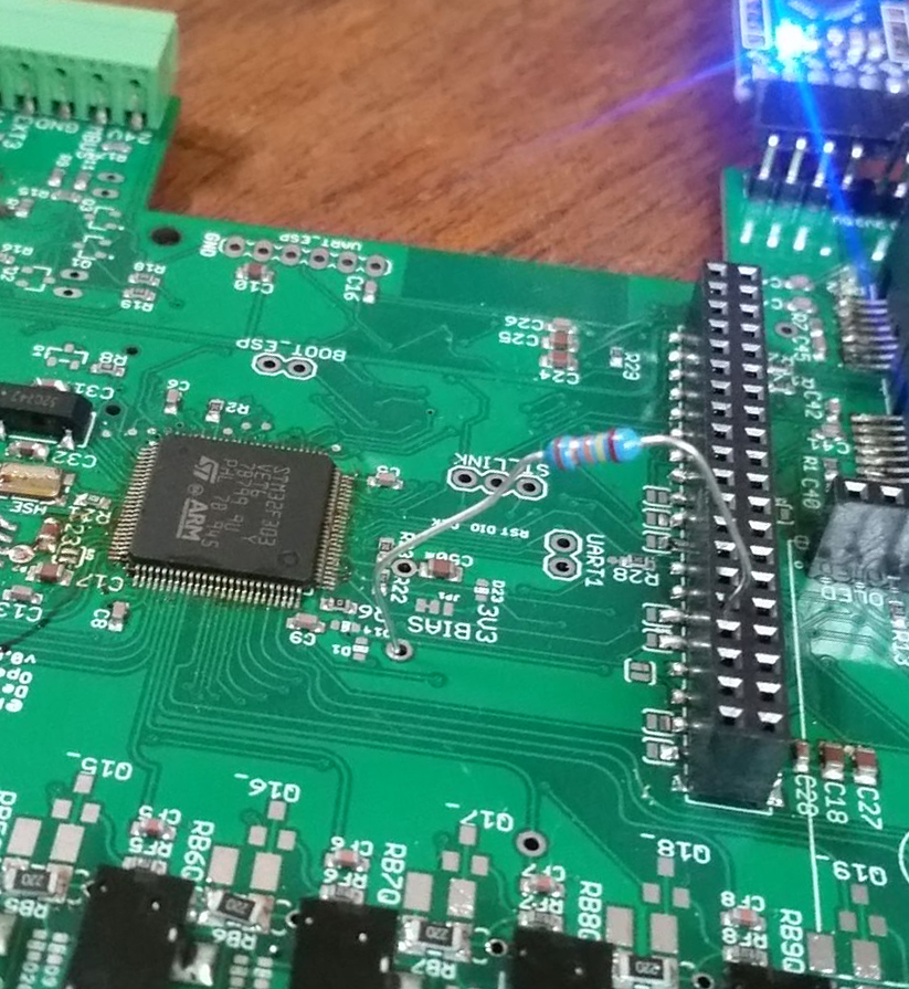
To completely change the subject, what’s the CANbus used for?
I don’t know, I just broke it out.
That is probably to most random thing on the board 
@Robert.Wall I’ve looked at few example applications of virtual ground this morning and we do have something different. I had to look at a few more circuits. Throwing out the virtual earth term here and we can just say the bias is being used as the ground connection of a vt or ct.
It gives people the wrong and misleading information when you use an established term to describe something completely different.
Agreed. I can only try be more careful.
What’s intended to plug into the 3-phase voltage inputs? I ask because the R53/R43 divider on the single phase V input forms part of the LPF. On the single phase input you’ve got a 18k2/10nF filter but on the 3-phase inputs you’ve got a 9k1/10nF filter. Was that intentional?
Also, you might want to consider moving protection diodes D22/D23 to the other side of R29.
And I think you can lose the protection diodes on the output of the opamp. What do R6, C35 and C36 do (and what’s the value of R6?).
I’ve tried this on the user side for a terminal block https://uk.rs-online.com/web/p/pcb-terminal-blocks/8971017/
That R26 on the single phase, good spot, it was left over from some trying to make the input more versatile but forgot to get rid of it. I’ll make it 0R for now.
I moved the diodes for the other inputs to the correct sides so this one must’ve got away, changed.
The R and two Cs on the opamp output are for testing. The bias trace with passives only (not the above three components mentions) measured around 25nF. I was going to try use the feedback components to counter this. I’ll have to read up again on how to quantify that. Any tips?
I found ±5% caps for all the filters, lower than that and they became quite expensive.
R29?
But if you make R29 0R there’s nothing to move the protection diodes to the right of.
What’s the exact problem you’re trying to solve there?
Yes, that one ![]()
True!
I found in testing the previous board that adding capacitance to the bias line increases noise. The idea is to counteract any existing capacitance on the bias line. I don’t know if there’s anything to be gained from trying yet. I see the opamp characteristics on the datasheet, a 50pF capacitive load is a maximum it seems.
Ah ok… yes, I see now that BIAS line is quite loaded with all those inputs. You could try hooking up an external tranny to the op-amp output. Have a read of these (there are 3 distinct URLs there but the forum s/w has pre-viewed just one):
https://www.edn.com/simulation-shows-how-real-op-amps-can-drive-capacitive-loads/
They look useful. I’ll look into them in detail tomorrow. Noticed from a few places now this circuit is quite common.
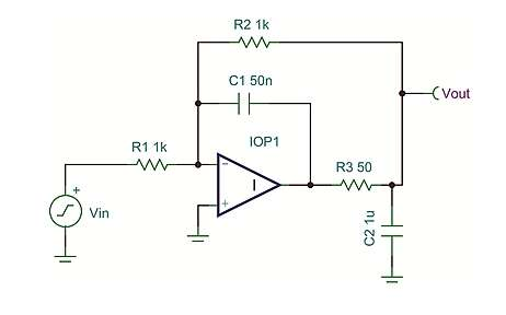
My schema was slightly different to this, I’ll look to make the change, which is to connect my C1 directly to the output instead of being in parallel with R2.
It’s actually completely different. Inverting as opposed to non-inverting too.
I could commit to the inverting topology. If that was the case, then I’d set bias at half 3v3 through a gain of 0.5 instead of the 10k/10k divider, assuming no knock on effects are made which can’t be dealt with further on.
Working my way through some pieces of the puzzle…
So far I’ve realised firstly I need to know the source impedance of the opamp.
Then I can get the dominant pole at this approx 25nF capacitance I measured (checking again on my bench meter it’s 27nF).
1. Impedance measured following this one.
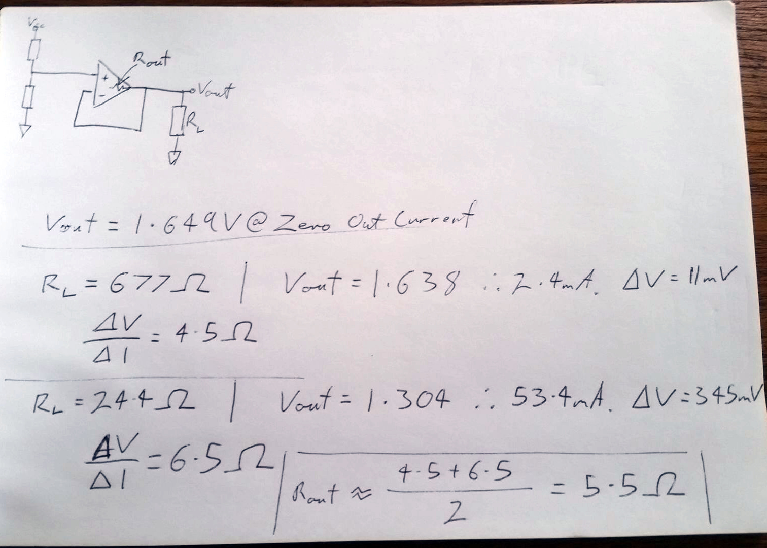
2. Dominant pole
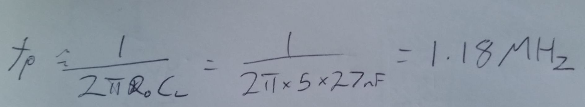
Using 5.5Ω it’s actually 1.07 MHz.
3. Stable?
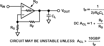
Image source.
Acl = 1 because we have a follower in the previous design.
10GBP = 82,000,000
fp = 1.07MHz
82/1.07 = 76.6 … This result suggests we had an unstable circuit before!
4. Feedback capacitor
Finding the value of C1 from the circuit in my previous post… some notional figures are:
source 1
1.5nF ballpark value if it’s follower instead of a g=0.5 system.
source 2 the article at EDN.
2.7nF ballpark, R3C2 = C1R2 suggested, and the author then goes into detail on why it’s not that simple.
I think at this point I’ll be able to go ahead and make up the ‘in-the-loop’ compensator in the board design so we can get this next iteration out. I might need some help to work out the values mathematically before they arrive, or if I need I’ll be able to do it experimentally I’m sure.
That does look like a neat trick, perhaps I’ll get the footprints on for jiggery pokery. I’ll come back to this one as just getting my head round all these phase margins first.
I hope I’ve not led you astray here. The sole purpose of my post was to show how you could use a transistor on the output of the op-amp to better drive a capacitive load. I’m not sure what problem you’re trying to solve with all your other changes.
Not at all. I was looking at a compensator before. I’m feeling on top of it now. I’ll be able to report back with some figures when testing the next revision. I have footprints on for testing a few options, including transistor. Can you recommend a sot-23 tranny? I have these at the lab https://uk.rs-online.com/web/p/bjt-bipolar-transistors/8064642/
The problem was noise and bias instability. Much of this will be sorted out by separating grounds and 3v3 lines anyhow.
A few proto-boards are out for manufacture. Changes since v0.9a:
v0.9b changes
- single phase input filter, R26 set to 0R.
- opamp with footprints to try out-of-loop compensation (single resistor, or snubber) and in-the-loop compensation, also with sot-23 transistor footprint.
- 2.54mm header jumpers included for switching in or out the burdens ( voltage output CT compatibility ).
- ac-ac input has footprint for 1210 burden smt. might give an option at loading the ac-ac adaptor to get a slightly more accurate representation of the mains signal.
- reference voltage set at 2.048V.
stm32 v0.9b.zip (1.2 MB)
Initial testing should be done by September. We’ll discuss in-house what we find and likely share much of the test information this time, cross fingers it should be looking alright.
I found a way to share the enclosure design.
There’s an option there to download the step file also.
We have a few PCBs assembled for this v1.0 stm32 prototype if anybody’s interested.
The assembled PCBs are £54.60 each, this includes a small markup to cover assembly time.
They are compatible with existing emonTx/Pi sensors. With small modifications they can also support voltage output CTs and voltage sensing transformers.
The code for the 3-phase voltage input has not yet been done, but if someone has a way to test it this is something we could discuss.
I can also get enclosures 3D printed for £35 each, or I can share .stl/.stp files if you’d like to use another service.
Many thanks.
Edit: RaspberryPi header not shown in the image there, but all units will have the header to be able to mount a rPi also.
Edit Edit: Now included in shop for easy purchase. https://shop.openenergymonitor.com/stm32-energy-monitor-dev-board/

On some tests I did a while back I found that the bias line for the current transformers had to be a really low impedance otherwise large signal inputs could modulate the bias line and then affect all the other channels that are sharing the bias line. One option if this is a problem is to add a separate RC filter on the bias line to each CT and that way signals on one CT will be less able to couple through the bias line to the other CTs. Hopefully this will not be a problem for you on this design.
Also, is op-amp offset voltage drift with temperature an issue that needs to be worried about? It may not be too much of a problem if the bias voltage drifts a little. It would certainly add a lot more cost to have a separate zero drift opamp if this was a problem.