Actually Robert, Bill had provided exactly the information on Cable I was interested in.
I’ve had a look at those manufacturers also, interesting stuff.
I’ll pick up other points later.
Many thanks.
Actually Robert, Bill had provided exactly the information on Cable I was interested in.
I’ve had a look at those manufacturers also, interesting stuff.
I’ll pick up other points later.
Many thanks.
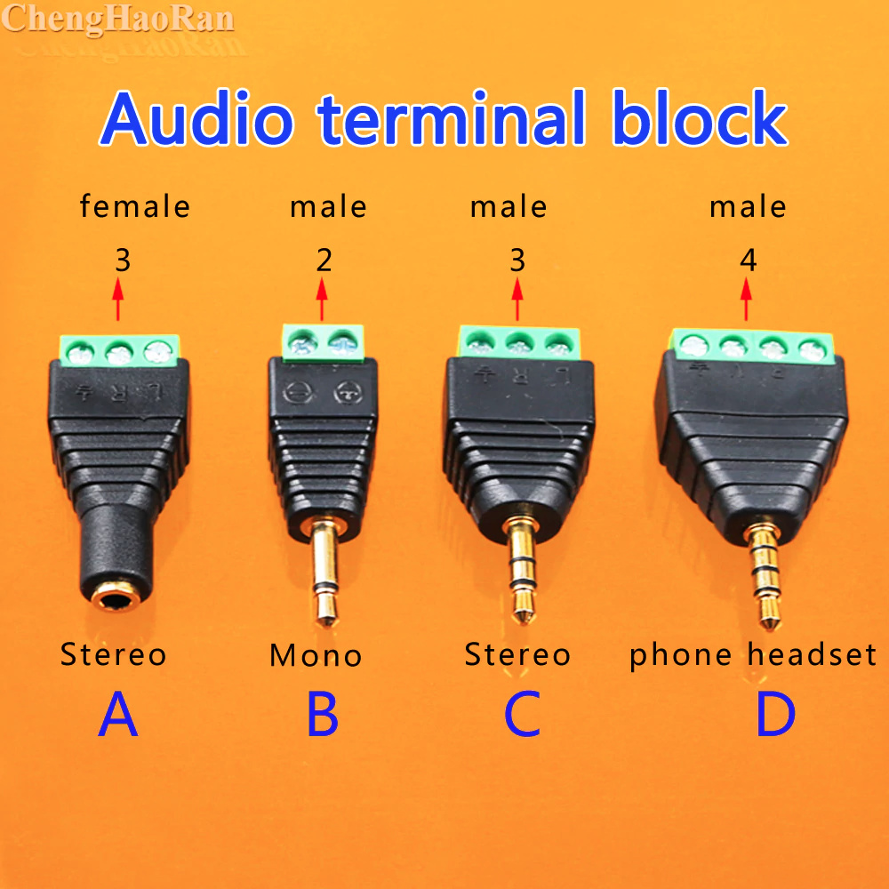
It’s good to have the wire AWG information regardless 
These plug breakouts accept 26-16AWG.
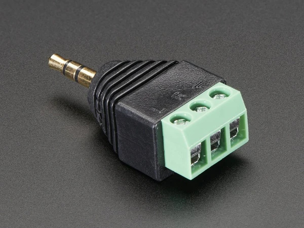
Who has an opinion on these?
@Bill.Thomson Edit: I’ve ordered one to get a feel of the quality.
@pb66 Can you use eagleCAD? The files are available if you’d actually like to have a look and comment on specific elements. Pretty much all of what you’ve mentioned has already been thought about or discussed in the lab.
I don’t have a table of pinouts, connections or capabilities I can post here now because we’re developing, testing… however this will be a natural part of the documentation.
Elsewhere…
You’ve already had “thousand and thousands of pounds” worth of help from @dBC on this project, so how about putting some of it back into the system? Isn’t that what Open Source is all about? ![]()
Turn it up everyone.
It seems they do not really come in a robust form (which I was looking for), just bare board.
Nah, I’m way cheaper than that ;-).
 Don’t tell everybody that.
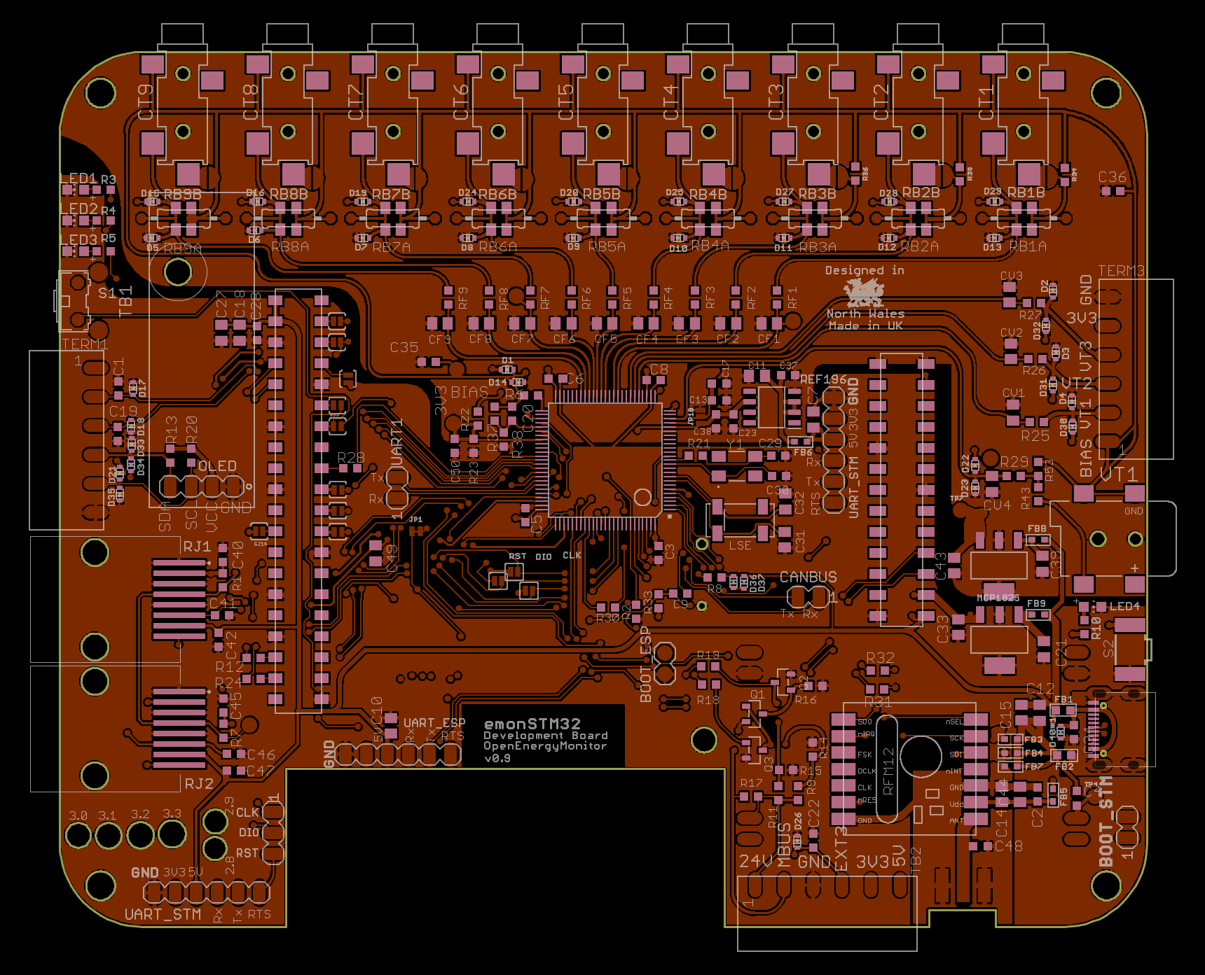
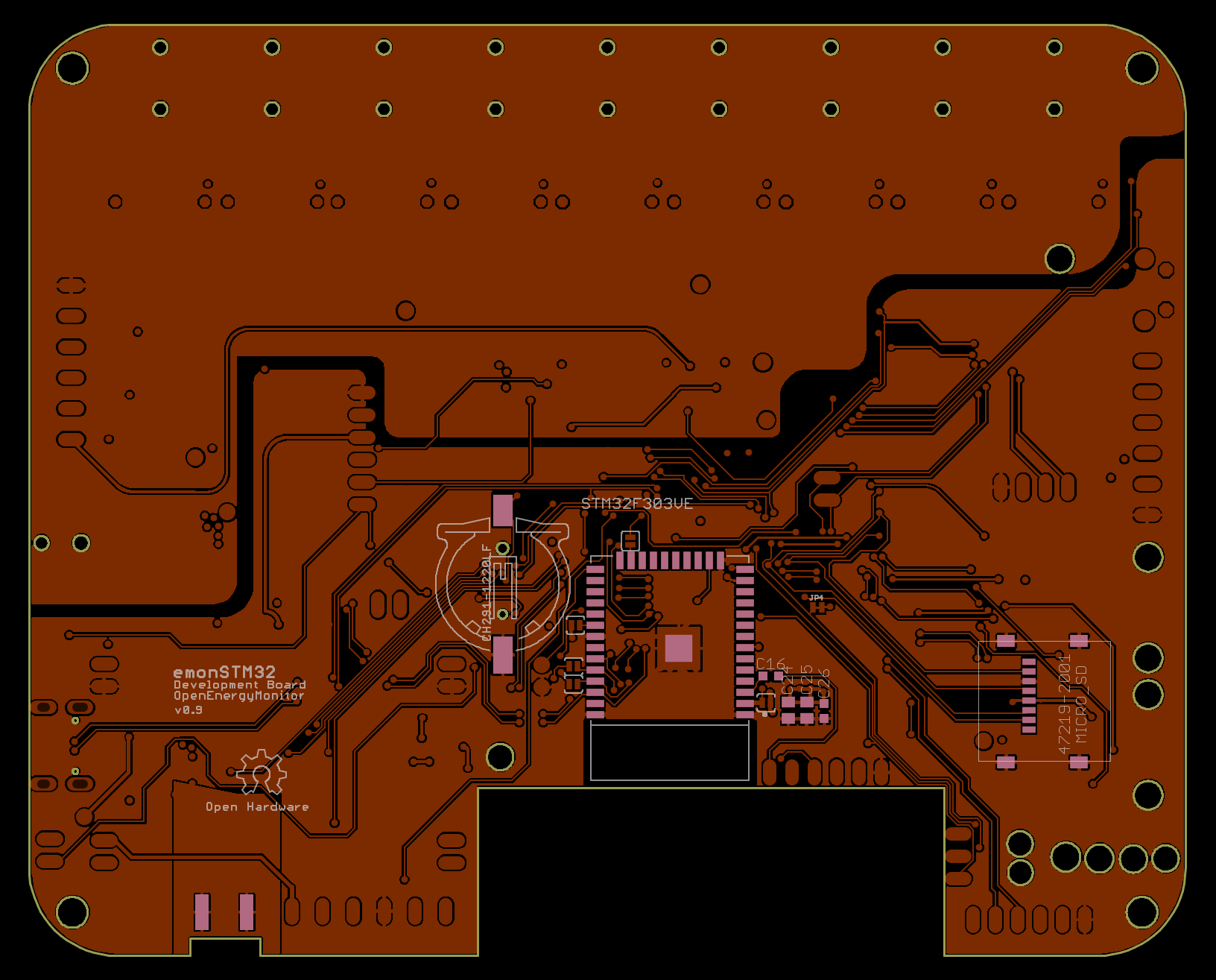
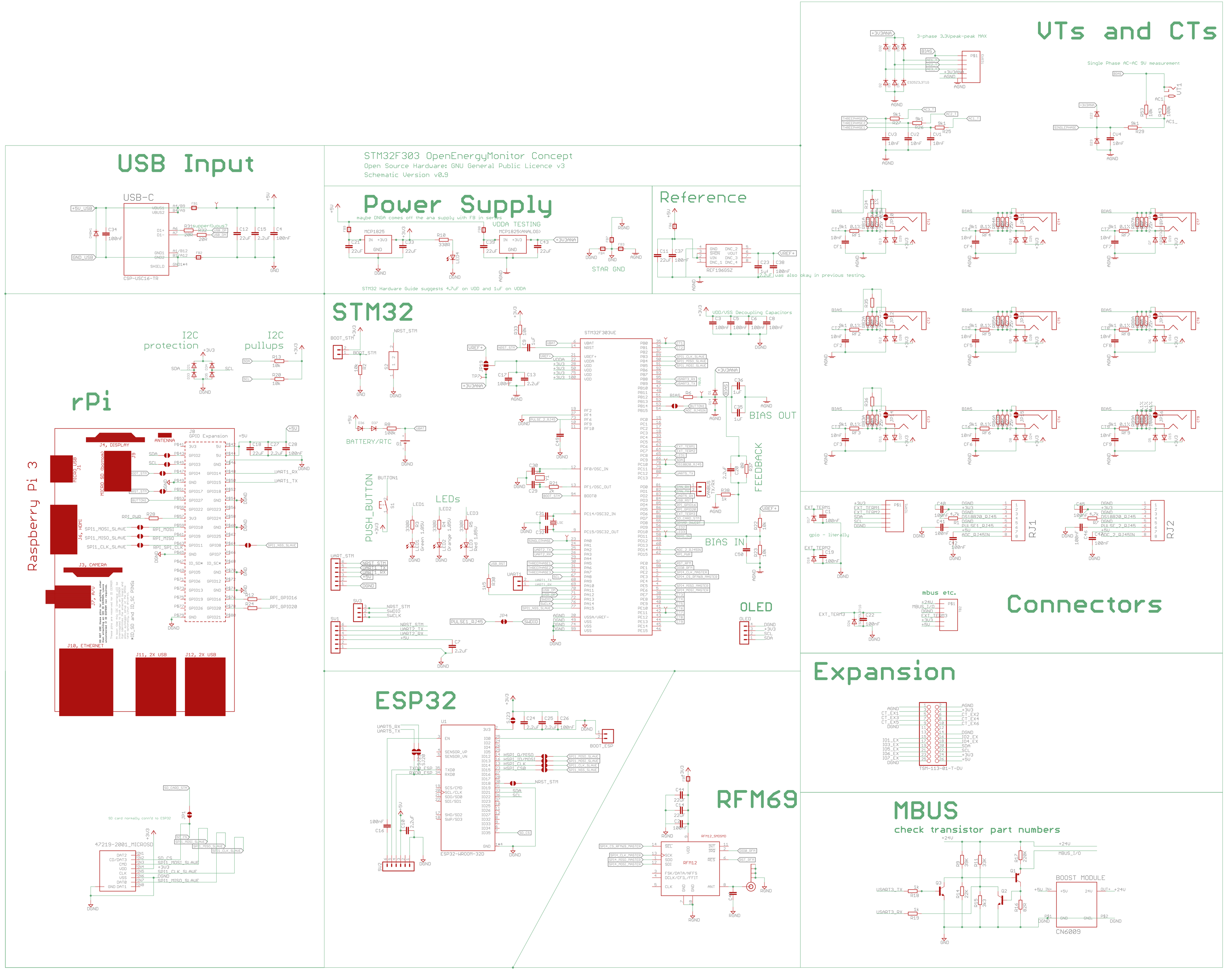
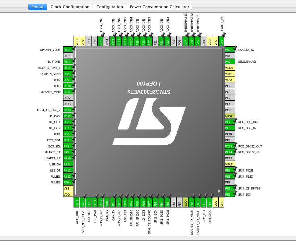
Hello everyone. Here’s the latest iteration of the stm32 board. Discussion welcome.
Full Gerbers and eagleCAD - stm32 v0.9a.zip (1.6 MB)
Changelog for this version below.
v0.9 main changes
design to do:
cubeMX(v4.2.7) file also: Sombrero_VE_Working5.ioc.zip (5.8 KB)
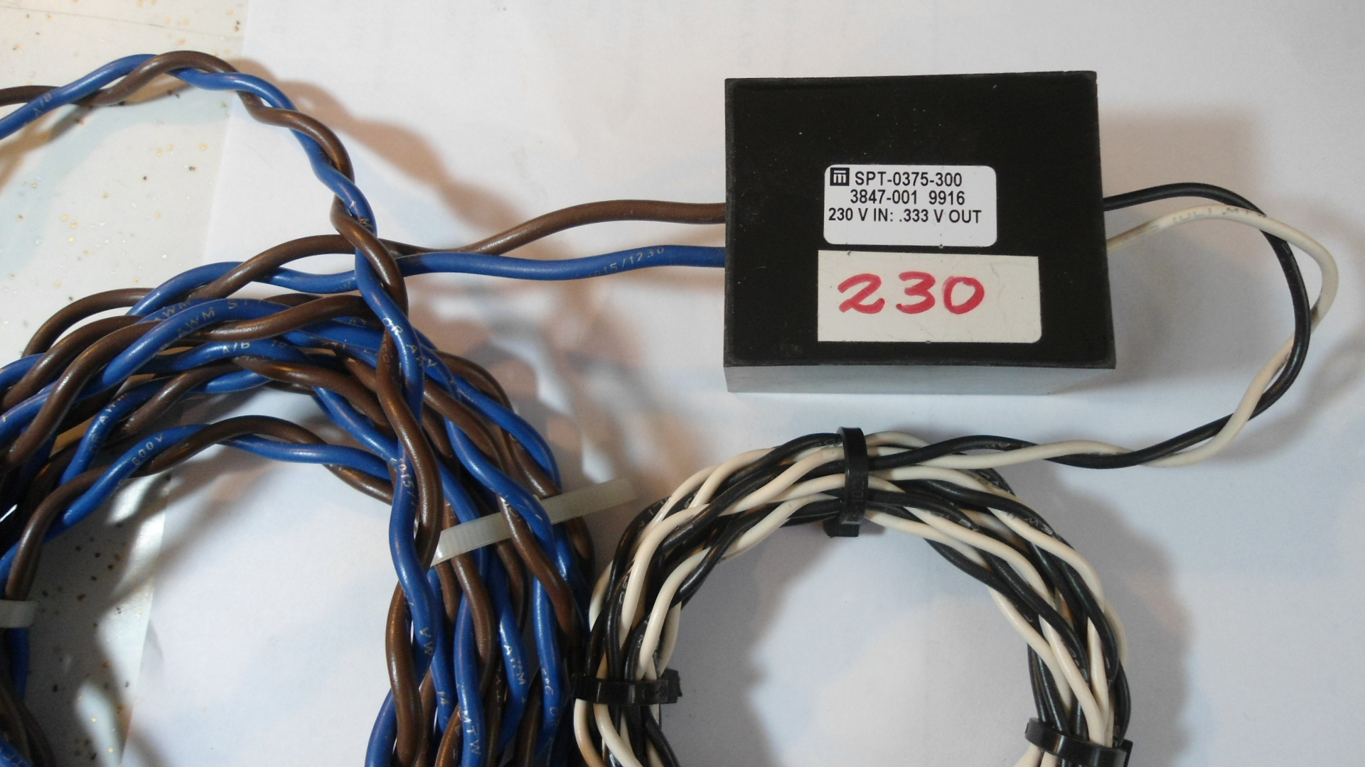
Looking at the voltage and current inputs, would I be right to think that you are keeping the rather non-standard - as far as measuring instruments are concerned - 50 mA input for the current side and 12 V rms (from a nominal 9 V source) for single phase or 1.1 V rms for 3-phase for the voltage side?
If so, you are preventing the use of the standard and very widely available (and accurate) 0.333 V rms output c.t’s and rather less widely available but accurate v.t’s. For a justification of “very widely available”, especially for c.t’s, a Google search for the two types will suffice.
You might like to read this from a US c.t. manufacturer: Current to Voltage vs Current to Current Transformers Magnelab
This is not to say that the existing OEM practice should be abandoned, but that I think consideration should be given to make it easy for the user to use either, by a method that doesn’t require an excessive level of knowledge either in electrical engineering or in the product.
We’ve come away from a discussion on this subject just now, so it’s confirming to read your comments, the article too.
I’ll take this point about the voltage output CTs seriously and read further. We should get some for testing…
The other point raised in discussion easier is that many voltage output CTs are 1V output, thus, we could change the range of the Analog Reference at the stm to suit, for better accuracy.
I can’t find reference to a 333mV device for the 3phase voltage inputs… The inputs should be okay in theory… The BIAS, GND, and 3V3 are available along side the voltage inputs. Whether the physical form of their availability suits practical use or not I can’t say for sure…
From what I’ve seen, the 0.333 Volt type are much more common than the 1 Volt type.
Magnelab, Byram Labs and the others that offer the 1 Volt units, offer them as an option
that typically costs more, and incurs additional lead time to manufacture them.
The 0.333 Volt devices are a standard stock item that Magnelab et al have available for
immediate shipment.
In terms of our design here, the difference I can see this making is in the chosen ADC range, i.e. the chosen reference voltage level.
And don’t forget, Magnelab’s precision v.t. is also 0.333 V output.
It seems as if one of the output leads of that transformer can be connected to the BIAS line as a virtual earth the other lead of course connected to one of the three voltage inputs.
It’s not a virtual earth, it is an earth to alternating currents – an a.c. earth is how it’s usually described. A virtual earth is one that is maintained by the feedback action of an amplifier.
If you fail to reduce the ADC reference and the bias point appropriately, then you are using just one third of the available input range of the ADC. That won’t be significant with a voltage input that can be expected to remain within 10% of the nominal value, but using only a third of the range of a current input effectively means that the current below which the measurement accuracy becomes unacceptable is three times higher.
I think the minimum allowable Vref on that processor is 2V so you’ll be stuck with half the available range.
If you were thinking of VREF+, that is indeed 2 V – VDDA. Even then, that at (say) 2.048 V is better than a 3.3 V reference, given 1 V p-p outputs.
Understood. This is an earth to the AC. I can see where the virtual earth at an op-amp is a clear and useful definition, however I was using the term more loosely as a rail-splitter (I’ve just read the wikipedia).
Developing on this understanding, with respect to virtual earth purely at the non-inverting op-amp input, it would be correct to describe this application more fully as a ‘virtual earth to the AC transformer’, as it is maintained by bias which is sourced from an amplifier, thus it’s sourced from a split rail.
As a side note, I have set the op-amp in this latest version as, not a follower only, but as a standard op-amp, I have footprints enabling myself in the next round of testing to explore using feedback to reduce noise and oscillation noise if necessary. I can of course use the voltage divider input to the non-inverting input to scale down the bias to a level compatible with any CT/VT system chosen. It’ll be a matter of testing…
@dBC I was going to mention this next, the datasheet recommends a minimum vref of 2V for this stm. I believe, for no particular reason, that it can go lower than this, but that is the recommendation. So happens the ref19x reference I’ve chosen has it’s lowest variant at 2.048V. The footprint is compatible with the LT1461 the lowest option of this is 2.5V.
@Robert.Wall Seen your latest above just now.