Ok. The MCP3008 does have an internal separation between the analog and digital grounds, so I may not need to be overly concerned with it.
Unfortunately, the datasheet for the MCP3008 isn’t that detailed. It just says:
A bypass capacitor should always be used with this device and should be placed as close as possible to the device pin. A bypass capacitor value of 1uF is recommended.
BUT…it continues to talk about the ground planes, and it says if no ground plane is utilized, both grounds must be connected to VSS on the board. Is VSS in my scenario the Pi’s ground bus, or pin #2 of the LMV321? So if I can determine which ground is VSS, I can infer where to connect the filtering capacitor to.
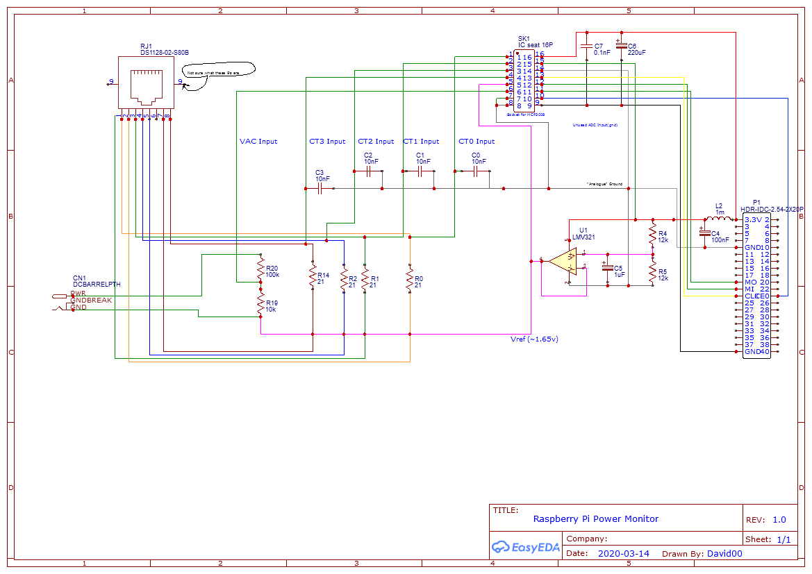
Good catch!! I think I’ve managed to correct L1 in the latest iteration - and the others too.
Got it! This publication is also referenced in the MCP3008’s datasheet. I will review it.
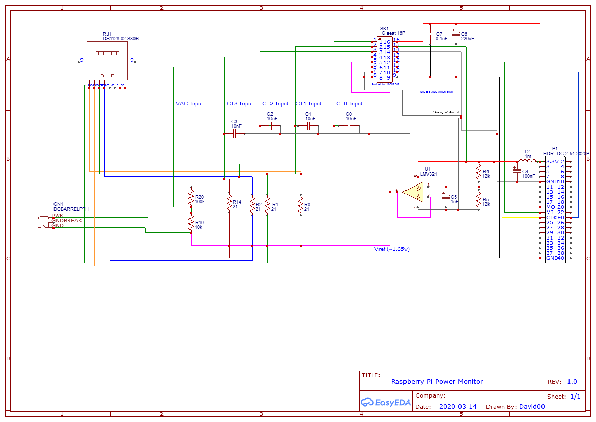
You know, now that I’m using the operational amplifier to supply the bias voltage for all 5 individual circuits, I should be able to fit the entire project on a single perma-proto board. I did order extras of everything just in case there were substantial design changes like this… so that might be worth a try before the custom PCB.
so you would do better to respect and use it if you can.
This is a bit chicken-and-egg. It depends on where and how the two grounds come together. How you need to be thinking is: Where does the current with all the digital switching transients etc - from the RPi as well as from the digital side of the 3008 - flow, and how can you best keep them apart?
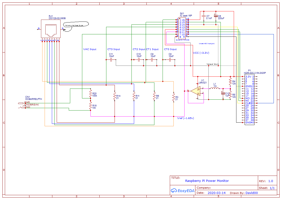
The LMV321 definitely needs to be regarded as part of the analogue side, so pin 5 (VCC) needs to get its supply from the clean 3.3 V, and pin 2 (GND) needs to go to the clean analogue ground. Otherwise, the mid-rail reference will have noise on it, rather defeating the object.
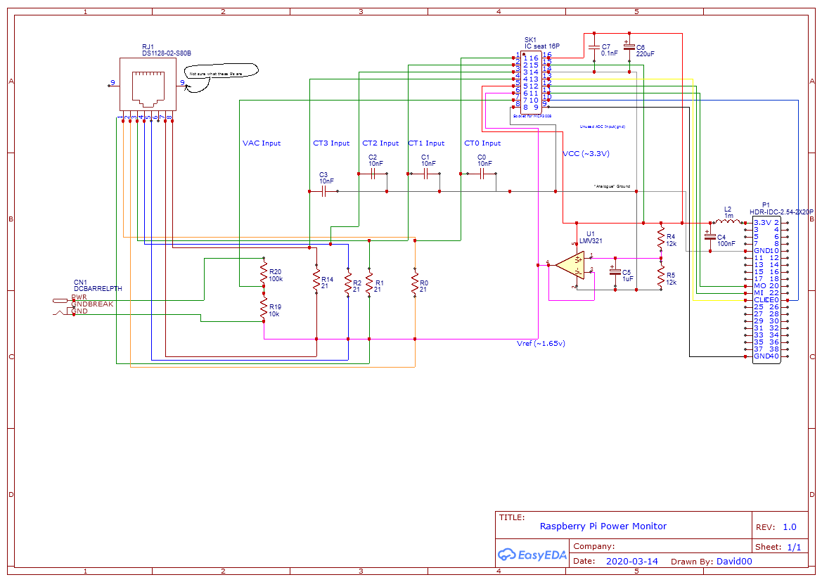
Argh! You’re going from bad to worse. L1 is completely in the wrong place now.
Let’s (conceptually at least) start from the beginning. Your 3.3 V comes from a dirty pin on the RPi and there’s a dirty ground that goes with it. Those two pins need to feed the dirt-generating dirty digital part of the 3008, i.e. pins 16 & 9.
From the dirty (pin 1) of the RPi, you need to take a feed for the analogue circuity and clean it up. You take it through your LC filter and use it to feed the clean analogue side of the 3008 (that’s AREF), the Op.amp and its input divider; and those plus all the analog smoothing, filtering and decoupling return to the clean analogue ground. If you have a clean analogue ground on your RPi, it connects there. Otherwise it connects at one place only to the common ground, and preferably as near to the source of power as possible, so that there’s no digital dirty current flowing in a wire or trace shared with the analogue return current.
1. You’ve lost the analogue ground to the op.amp and the 3008 AGND.
2. I’d still connect the VDD of the 3008 (pin 16) to the dirty side of L2, otherwise you’re putting digital noise from it onto the clean analogue power rail. Likewise now that you’ve separated the analogue and digital powers, C7 & C8 need to return to the digital ground on pin 9. Depending on how exactly you lay out your PCB, you need to consider the last bit of section 6.5 of the 3008 data sheet. That infers that noise can enter the 3008 via the digital ground pin, and that will be worse than the 3008 injecting noise into everywhere else. This might only be true if you have a substantial ground plane.
3. There’s no point in taking the 3.3 V to the ADC to measure it, it will only ever read full scale (1023), because that input pin will be the same voltage as the reference, and 1023 counts by definition represents the reference voltage.
Is it not still there? It’s pin #14 on the ADC going to pin #9 on the Pi header. The routing in my schematic doesn’t look like the routing in the schematic of the Learn section, but I think the connections are still the same.
That makes sense. Thank you.
That is the next challenge. The layout of the parts is tricky. I’ve experimented a little bit but I know I need to review the Microchip document you suggested before committing to a layout. I would prefer to follow the Pi HAT specification which restricts the board dimensions to 65 x 56.5mm. The components look like they’re fit nicely with plenty of room, but I think routing the traces efficiently in only 2 layers is going to be difficult for a first-timer like myself. Maybe I’ll have to do a 4 layer and put the analogue grounds on its own layer.
I see - I think that was leftover from my original implementation where I was originally sampling it. I had commented it out in the code, but not removed the circuitry for it.
Here is the updated schematic after moving the VDD to the dirty side of the 3.3V supply, and the filtering capacitors to the digital ground of the MCP.
Is there a join where the vertical line from pin 2 of the op.amp (Vss) crosses the GND from the RPi? If there is, that is what threw me. Your drawing package is faulty, you never, ever have a 4-way join on a diagram, and it shouldn’t have allowed it. I read it as a crossing.
I thought I should note it. That’s a few less components to lay down and a few less tracks to route.
Pin 9 on RJ1 is probably mechanical fixing for extra strength as much as anything. Look at a photo and they’re the metal screening can.
Great! I am beginning to study Microchip’s layout tips so I can refine the layout some more. I have already toyed around with it since I found it somewhat fun, but it’s probably not that great.
One general question I have off the bat is since I’m using through hole components for everything (except the LMV321), do all the “pads” for the components need to be on the bottom layer of the PCB?
No - but it’s not good practice to have just one pad on the front - because it’s only the glue bonding the copper to the substrate that is supporting the component. On the back you really should have a ‘blind’ pad that’s not connected anywhere but it prevents the lead-out wire pulling through the board and the part falling off, taking the front track with it.
If the holes are plated-through, then you don’t need to specifically solder both sides, the solder will run through. If you don’t have plated-through holes, you must solder both sides to give you a secure mechanical fixing and an electrical connection.
Thanks for the guidance! I’ve studied the Microchip AN688 guide and I think I have something worked out. I also found this helpful in learning the basic circuit-board technology.
The Microchip guide really seems to be pushing for a ground plane so I’ve incorporated one into my design on the bottom layer. Before today, I was under the assumption a ground plane had to be in its own layer, which was why I was thinking about the 4 layer board. After catching up on what feels like a semester’s worth of information, I’m hoping I’m close to being ready to submit my order for the PCB.
I have adhered to the design principles in the AN688 guide to the best of my know-how. Also, despite the guide’s suggestion to not use the auto-router, I did, with the hope that auto routers have improved since the document was published around 20 years ago.
You can view the layers directly in the web editor at the link.
Some factors I considered in the design were:
Power traces are 2x as wide as signal traces (12mil and 6mil, respectively) Question: Should I make the main ground traces the same size as the power traces? My experience in car audio is telling me they should be the same.
All analogue devices are kept on the “analogue” side of the ADC
The only trace running under the ADC is the ground
Traces are as short as possible, while trying to maintain some level of organization.
Also, when I do move away from the first iteration of my project (the 2 stacked perma-proto boards) and onto this 2nd iteration (v1 of the custom PCB), I am going to remake my CT cable. I bought some shielded Cat6a to replace my UTP Cat5e. My CT sensor lead is running through about 2 feet of flex tube… right next to a 240V line I installed last year, so there may have been some EMI involved in the CT sensor lead. I’m hoping the shielded cable helps to keep that out. The 240V line is energized, but nothing is consuming power, so there shouldn’t currently be any EMI, right?
On another note, I hope you all are staying safe up there! Las Vegas is very strange right now with grocery stores wiped out and the Strip gone dark.
I won’t have time for maybe a day or two to look at your layout in detail - I’m quite certain it will be an improvement on the plugboard/protoboard - past experience here tells me that those physical arrangements have always been more susceptible to noise etc giving rise to ‘phantom’ currents.
Yes, I’d make the ground traces as wide as conveniently possible, so that volt drops are minimised.
And again, screened cable should help, if you get it right and don’t introduce ground loops. I.E, ground the screen at only one end.
Wrong. You’re only thinking of magnetic fields. If there’s capacitive coupling and voltage spikes, the electric field around the cable will transfer charge, which the screen should deal with. Hopefully, but don’t dismiss it too quickly. If you can separate the two, so much the better.
I have been thinking about this and several options have come up. I just revisited the cable extension section on this site for some guidance. My options are:
Ground the cable at the end that’s connected to the Pi by: running a small conductor parallel to the Cat6A cable (about 10ft) into the electrical panel and attach to one of the many grounds in the panel
Ground the cable at the end that’s connected to the Pi by: running a small conductor to the nearest AC outlet and using a grounding plug (~ 3-6ft away)
I’m leaning towards the longer run into the panel because I don’t really want to tie up an AC outlet with a ground, and the ground plug I’ve found is ridiculously priced for what it is. I would rather wire my 22 gauge wire into a standard nema 5-15p plug and save the money, as silly as that would look. Plus, I can package the Cat6A and the grounding conductor in a braided sleeve so it looks like a single cable.
Or, should I just ground the cat6a sleeve at the end inside the panel and save the long grounding conductor run?
No rush in reviewing the PCB. I have to review it too - I was up way too late last night working on it which means it’s extra likely that some errors were introduced somewhere - perhaps even from the schematic. Thanks!
Yes, the main panel has a ground bar which is connected to the grounding rod.
It’s probably more like 5ft, but my Cat5e cable will probably be 8-10ft to give me some flexibility in where I place the Pi. I have a short conduit from the electrical panel to a 3-gang box inside my garage where I intend to place the Pi on a shelf. I could place the Pi inside the electrical panel, but my main concern with doing that is Wi-Fi attenuation inside the metal box.
The Pi’s power adapter is only 2-prong (hot and neutral), so there’s no real ground there.
I’d be inclined to ground the cable screen at the ground busbar, and at the other end connect it to the Pi’s GND, or better still if the Pi and your board is in a partially screened box, to the screen. That is something you can play around with when it’s set up.
(The emonPi is in an extruded aluminium case, but the end where the WiFi is, is acrylic, to let it communicate. You could do something similar.)
Don’t know how you are with NEC code compliance, but if you want to keep it “legal” then you need to
run the low voltage wiring in its own conduit. NEC says running HV and LV wiring in the same conduit is
a no-no.
Like the HV/LV wiring scenario, this one is also not cool.
AIUI, the only other item that is OK inside a load center, aside from the hardware that’s intended
to be inside an LC, is a CT. Even then, the CT wiring “path” i.e. conduit, flex, etc. is not supposed to be shared with HV wiring. A shared path with other LV wiring is OK.