Warning - JLCPCB & Module V4.40 and part D2

I feel like there are letters all over the silkscreen. I’ve also tried pluses and little arrows, they weren’t as clear for me.
Also that leaves some space if I wanted to say what color the led was/is.

If you are wondering, I’m making the new controller board easier for me to assemble and use. It’s still in progress though. I’ve moved the vias that were directly on top of a pad and gave some tracks a little breathing room along with changing the jst-ph connectors.

not difficult to solder
yes on a new pcb

managed to unsolder only with two soldering irons heating both ends of D2

then rotate it and it wont lay flat on the solder joints because of old solder, so again two irons left and right and then it was in place

was very funny :slight_smile:

but now all modules D2 is stripe on the + marking of the board
waiting for the attinys and the new controller to complete the built

thanks for your help and your work for that great bms.

1 Like

It’s essentially half of the schematic symbol for a diode.
image

Hi @Fred7421, interested to see why you think the board is difficult to assemble - are you planning to do the whole board (SMD) by hand?

Why do the vias on pads cause you a problem?

The JST sockets are easy enough to solder 2.0mm vs 2.54mm isn’t much of a difference.

via in pad is sometimes charged extra by board manufacturers. JLCPCB and PCBWay do not charge for this from what I’ve seen though.

I think the difference here is the 2mm pitch connector is a bit more challenging for some people than the 2.54mm pitch. Though, there are a lot of off-the-shelf cables that can be used with little modifications (swapping red/black as example for module power)

I’ve updated the silk screen (again) today, don’t think I can make it any clearer than this!

image

4 Likes

For me, when I’m staring at the board…and the schematic…and the parts list; trying to figure out which part goes where is easier for me not to add to that confusion with which way does the diode go… what color led goes where… etc. It is just easier for me.

From digikey I’m using 2057-mts-02-ND and 2057-LHS-02-TRA-ND for the 2.54mm connectors. They are very easy for me to use. No reverse plugins.
Also It’s not that hard for me to modify the pcb layout in Kicad.

It’s another possible problem spot I choose to avoid if I can.

Indeed. For me I make my own cables and making the jst-ph connectors is no fun at all. Also plugging them in and removing them is no fun either.

Oh, I do agree with this. Still the JST’s are in use now, so no easy path to move away from them.

Premade cables is the way forward!

:smile: I wasn’t suggesting you change anything, I’m making it a ‘user-friendly’-‘build-it-yourself’ board for me.
I’d be happy to share it once I’m sure all is working as it should.

1 Like

Just received my PCBs from JLBPCB and my diodes appear to be correct. Now if I could just get Digikey to ship the other bits…

Well thats good news, glad to hear it.

Did they report it as rotated in the order page? I’m expecting my boards to arrive in a couple days and they indicate that they rotated D2 which is why I filed the issue on github and which sparked this conversation.

my v4.4 boards arrived today, I wasn’t expecting them until next week.

These boards have the D2 rotated (as shown in the GitHub issue) and based on a spot check on a couple boards under a microscope D2 is correctly rotated with the stripe towards the edge of the board (+ side). D2 stripe mark is rather challenging to see as it is more of a “cut” or similar into the top rather than like most diodes being paint/silkscreen.

2 Likes

Also just received mine today and my D2 part looks like @ChrisFullPower pic (the chip text is upside down relative to the DYBMS silkscreen text and thicker stripe towards right side of board). My order was placed on March 7.

1 Like

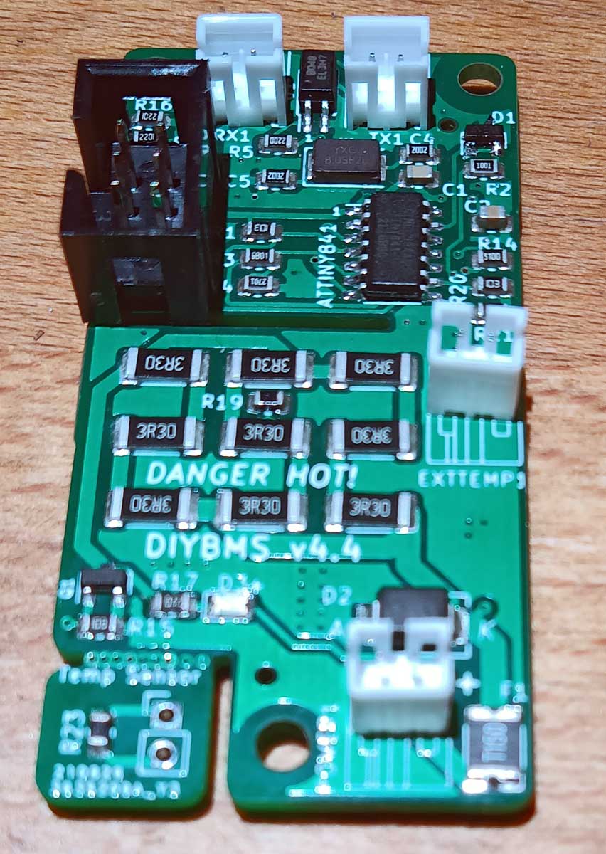
I got a batch of 20 modules from JLCPCB with 2 modules with wrong C4 and C5!
They place resistors instead…
So I recommend checking all parts carefully. JLCPCB is not reliable with placing correct parts.

This is the same error for the 4.5 modules, After a few back and forths with JLPCB, they are adamant the negative on the D2 part is the stripe and have recommended to remove the + marking and just leave the stripe marking on the PCB.

FYI I attached the images I found on the same github issue with the 4.4 modules to the chats with JLPCB, both the correct and incorrect images.

D2 isn’t needed to make the module work - worst case, they put it on backwards and you have to remove & resolder them all.

You’ll know if its wrong, as there will be a dead short across the power input terminals (so don’t connect to the battery!)