Warning - JLCPCB & Module V4.40 and part D2

I’ve had a few people contact me about V4.40 orders they have placed with JLCPCB.

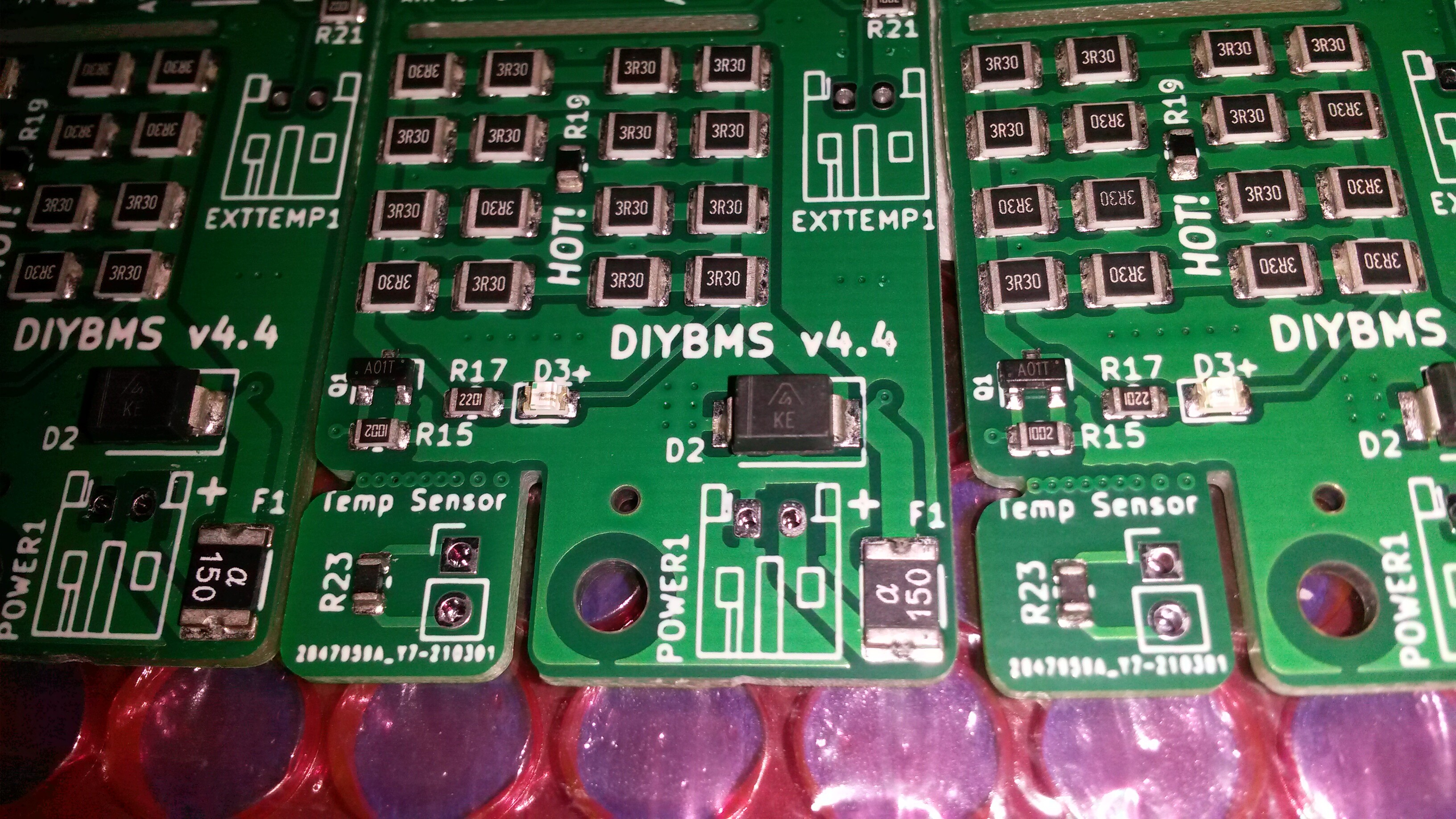
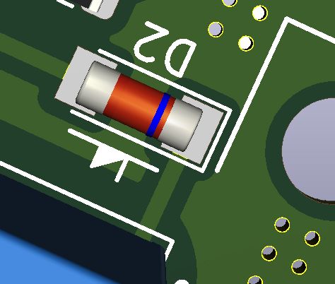
In production JLC are sometimes swapping part D2 around (rotating it).

If you have ordered from JLCPCB, please check any boards you have had made.

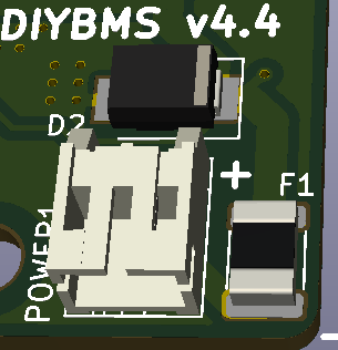
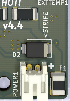
The D2 part should be like in the picture, with the “stripe” towards the right handside of the board, near the “+” sign.

Definitely check before applying power to the module, as an incorrectly orientated diode will cause a dead short across the terminals, probably leading to the fuse going, or something melting!!

There is also a GitHub issue open for more information.

Issue 73

If you do have boards which are incorrectly built, you have two options:

  1. Remove D2 completely (unsolder it), this also means you lose the “voltage spike” protection this part provides

  2. Unsolder D2 and rotate it, and re-solder it (recommended)

The part is quite large, so not difficult to unsolder with a normal iron.

A correct board looks like this:
image

2 Likes

@stuart
Wrong D2 orientation?
what do you think?

this is the ordered (first file with old resistors)

and this the delivered

1 Like

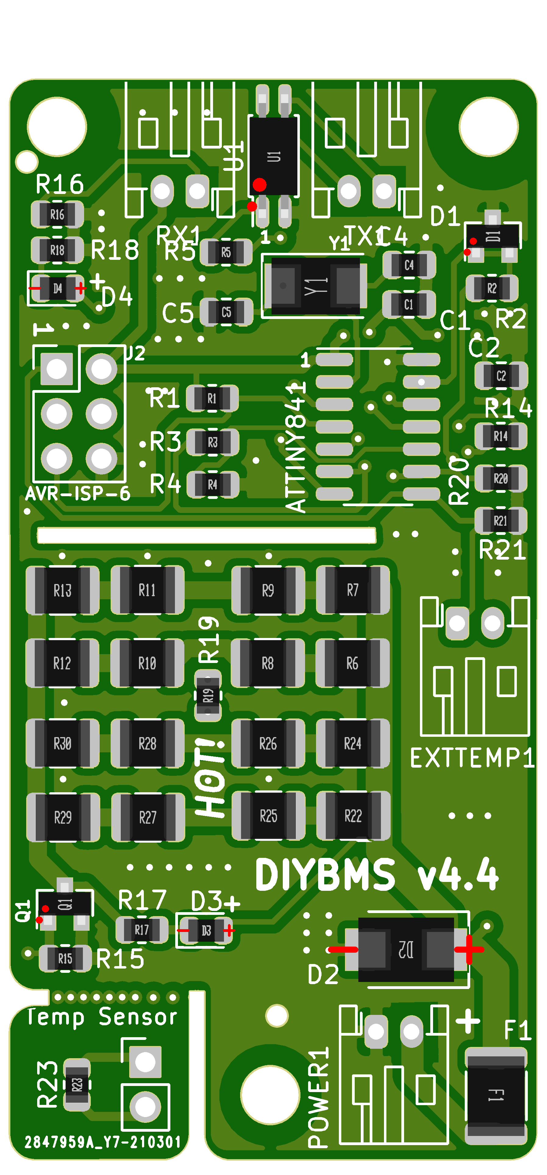
Looks nice, the temp sensor you break off then solder cables to the module itself i pressume ? I was thinking ordering a small board like that just for that purpose since soldering cables to a SMD component is just messy. What’s with the hole on the module ? For cooling ?

its the new version v4.4
watch stuarts video on youtube

Got it, i just looked it up in the repo.

THAT IS WRONG ORIENTATION!

DO NOT CONNECT THOSE MODULES TO ANY CELL/VOLTAGE!

You need to ROTATE D2 part - un solder it and rotate so the “stripe” is on the right handside.

Thank you for posting the pictures.

1 Like

@voltmeter can you tell me if the D2 part was out of stock when you ordered?

It seems that people are picking a different part, and JLCPCB have different orientations of that same part!

no it was in stock
was the original like in the bom file C440263
ive ordered right after your v4.4 video release

Thanks, unfortunately as per this forum topic, there is a lot of confusion on this particular part, sometimes JLC place it 180 degrees, sometimes zero degrees.

Unfortunately for you, you will need to unsolder and flip it over, or just remove it completely.

Don’t connect to a cell before doing this - otherwise it creates a dead short.

if i remove it, is the fuse stil working?

i think i dont need it because i have not higher voltage than 4.2V per module, if its higher then the module is not my problem anymore :upside_down_face:

The fuse is inline with the + voltage ahead of the diode. It will continue to work.

1 Like

It’s there to avoid spikes, electrostatic discharge etc. If you are going to the hassle of unsoldering it, you may as well just flip it over and solder it back on. Its quite a large part, so not difficult to solder.

1 Like

Just did a bit of research, these parts are meant to be similar, all marked SMBJ5.0A, all the same size/footprint (D_SMB) however when placed via JLC, the + and - is flipped!

C10204 + on right
C294856 + on right
C113974 + on right

C357965 - on right
C473804 - on right

I’ve just updated the PCB silkscreen to assist with a “stripe” marker.

image

1 Like

I use marks like this, it helps me place diodes leaving no doubt.DIODEMARKER

3 Likes

Good idea, is that a standard kicad footprint?

No I just made it up
I guess it could be made into a couple of footprints (left and a right)

Some boards use a “K” to indicate the cathode end of the diode… There are a few options for this likely.

I feel like there are letters all over the silkscreen. I’ve also tried pluses and little arrows, they weren’t as clear for me.
Also that leaves some space if I wanted to say what color the led was/is.

If you are wondering, I’m making the new controller board easier for me to assemble and use. It’s still in progress though. I’ve moved the vias that were directly on top of a pad and gave some tracks a little breathing room along with changing the jst-ph connectors.

not difficult to solder
yes on a new pcb

managed to unsolder only with two soldering irons heating both ends of D2

then rotate it and it wont lay flat on the solder joints because of old solder, so again two irons left and right and then it was in place

was very funny :slight_smile:

but now all modules D2 is stripe on the + marking of the board
waiting for the attinys and the new controller to complete the built

thanks for your help and your work for that great bms.

1 Like