STM32 Hardware Development

Easy I find, but a couple hours work perhaps making sure everything matches according to the datasheet.

Just to note, that for a new hardware project, it’ll be worth looking at KiCad, which I’ve heard has improved a lot recently, it’s open-source and doesn’t have board size restrictions.

1 Like

I’ve finally had a little time to look at STM32 hardware again :slight_smile:

First a good friend of ours and original NanodeRF designer who helped get OpenEnergyMonitor internet connected energy monitoring started: Ken Boak (https://twitter.com/Monsonite) has kindly shared a number of STM32 eagle files with us, perhaps the most useful design at this stage while learning about the STM32 platform is his ARMiGo design.

The ARMiGo is a 48-pin STM32F303 mini development board that includes basic power supply, ST-Link and USB connectivity. Ken blogged about the design in early 2014 here: A mini-ARM board, the ARMiGo | Wicked Device Shop

The Eagle schematic and board files can be downloaded here: ARMigo2_3.zip (132.8 KB)

Using this design and cross-referencing with the schematic for the nucleo f303 downloadable here:
http://www.st.com/en/evaluation-tools/nucleo-f303re.html and the pin-out reference accessible from within the STM32CubeMX application, Im slowly getting a clearer idea of what is required to put together a basic design.

I also realise that the easiest way to get the eagle components for the STM32 range is to use the STM provided bxl CAD fiiles and the recommended route of using the https://app.ultralibrarian.com online tool that can export these bxl files into a variety of formats used by common electronic design tools such as Eagle or KiKad.

stm32f303rxt (64-pin) stm32f303.lbr.zip (5.1 KB)

The CAD files downloadable from STM also include files for f303 100pin and 144pin designs. The xls file Select_BXLfile.xls details which bxl file to use.

My next step will be to read through the AN2586 and AN4206 application notes on getting started with STM32 hardware design.

1 Like

4 posts were split to a new topic: STM32 Calibration

ST-LINK JTAG/SWD Firmware Upload

The nucleo development boards come with an integrated ST-Link-v2 programming board that you can snap off.

The ST-LINK/V2 is an in-circuit debugger and programmer for the STM8 and STM32 microcontroller families. The single wire interface module (SWIM) and JTAG/serial wire debugging (SWD) interfaces are used to communicate with any STM8 or STM32 microcontroller located on an application board.

ST-LINK-V2: ST-LINK/V2 - ST-LINK/V2 in-circuit debugger/programmer for STM8 and STM32 - STMicroelectronics

M-07723

Alternatively you can buy cheap ST-Link-v2 programmers on ebay that avoid the need to add the full st-link programmer hardware to a STM32 hardware design. Ken’s ARMiGO design above has a 5-pin connector for programming with an external ST-LINK programmer.

In order to further my understanding of the hardware part of st-link firmware upload, I snapped off the st-link adapter on my nucleo development board and then following the pin out as documented on the schematic for the nucleo rewired both parts together:

Download the nucleo f303re schematic here:
http://www.st.com/resource/en/schematic_pack/nucleo_64pins_sch.zip

The 6-pin SWD connector can be seen on the left of the ST-link adapter board.

SWD

Pins

  1. n/a
  2. T_JTCK: Clock signal of target CPU, connects to PA14 on STM32
  3. GND, connects to GND
  4. T_JTMS: → SWD data input/output, PA13 on the STM32
  5. T_NRST: Reset → NRST on the STM32
  6. T_SWO: Single Wire Output → PB3 (Optional, not needed for firmware upload, used for output)

Then on the nucleo development board part, the schematic indicates the position of PA14, PA13, NRST, 3V3 & GND:

morpho_cn7

3V3 power for the nucleo STM32 board can be accessed from JP1 on the ST-link programmer.

Picture of the connected boards:

and firmware upload worked just the same as pre snapping off the ST-link board :slight_smile:

Serial/UART Firmware Upload
A second firmware upload method is to use serial (UART) upload, which works in much the same way as the standard way of uploading code to an Arduino. Like in the case of the Arduino serial upload this approach relies on a pre-uploaded bootloader. My understanding is that the Nucleo boards already have this bootloader in place.

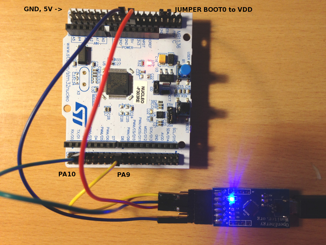
UART to Nucleo connections

  • Connect GND and 5V for power.
  • Place a jumper between BOOT0 and VDD to select the serial upload mode.
  • Connect PA9 to UART RX
  • Connect PA10 to UART TX
  • Power cycle to reset board and enter serial upload mode

Serial Uploader Tool

On Windows ST provide a tool for uploading firmware over serial called STM32-Flasher: FLASHER-STM32 - STM32 Flash loader demonstrator (UM0462) (replaced by STM32CubeProgrammer) - STMicroelectronics

For Linux there is a neat command line tool called stm32flash available in the package manager: Ubuntu Manpage: stm32flash - flashing utility for STM32 through UART or I2C

It can be installed with the following apt-get install:

sudo apt-get install stm32flash

I compiled the Arduino example Blink for the Nucleo64 STM32F303 using the Arduino IDE and then fetched the compliled .bin file from the /tmp folder that Arduino creates.

I could then upload to the STM32F303 by running:

sudo stm32flash -w blink.ino.bin /dev/ttyUSB0 -b 115200

Terminal output:

$ sudo stm32flash -w Blink.ino.bin /dev/ttyUSB0 -b 115200
stm32flash 0.5

http://stm32flash.sourceforge.net/

Using Parser : Raw BINARY
Interface serial_posix: 115200 8E1
Version      : 0x31
Option 1     : 0x00
Option 2     : 0x00
Device ID    : 0x0446 (STM32F302xD(E)/F303xD(E)/F398xx)
- RAM        : 64KiB  (6144b reserved by bootloader)
- Flash      : 512KiB (size first sector: 2x2048)
- Option RAM : 16b
- System RAM : 8KiB
Write to memory
Erasing memory
Wrote address 0x08002c5c (100.00%) Done.

If you are using the emonTxShield you can easily forgo all the link wires and use the serialusb programmer directly on the 6way header (see STM32 Development - #207 by pb66) by not populating the 5v pin and linking the 5v and 3.3v tracks on the shield. You also need to change a couple of links on the STM32 to access the uart via the Arduino headers, I can’t recall which now as it was a while back I did this, but it is documented in the nucleo user manual.

The blue user button can also be plumbed into the boot0 pin to replace the manipulation of a boot0 link wire with a button press.

A better option still is to use the GPIO of a Pi much like updating a rfm2pi (or emonpi) as then you can connect the boot0 to another GPIO pin and upload totally “handsfree”.

It is also possible to use the Pi GPIO to simulate an STlink and use the swd/jtag method without a STLink v2 but that’s more complex to set up and uses OpenOCD rather than the much simpler stm32flash.

Although ultimately I think it would be good to look at in-application programming for installing FW updates (not to be confused with communicating with the device for configuration, calibrating and debugging).

Thanks Paul, does upload work on UART2? RX and TX for the emontx shield are connected to D0, D1 on the arduino headers or PA3,PA2 on CN10 which are UART2 or did you have to do something else to configure?

My last challenge for the day was to test USB DFU upload, but I’ve been unable to get it to work so far, using the circuit in Ken Boak’s ARMiGo design.

Dmesg gives me the following:

[29399.151534] usb 3-2: new full-speed USB device number 95 using xhci_hcd
[29399.263613] usb 3-2: device descriptor read/64, error -71
[29399.479552] usb 3-2: device descriptor read/64, error -71
[29399.695559] usb 3-2: new full-speed USB device number 96 using xhci_hcd
[29399.807601] usb 3-2: device descriptor read/64, error -71
[29400.023537] usb 3-2: device descriptor read/64, error -71
[29400.239589] usb 3-2: new full-speed USB device number 97 using xhci_hcd
[29400.239772] usb 3-2: Device not responding to setup address.
[29400.443753] usb 3-2: Device not responding to setup address.
[29400.647576] usb 3-2: device not accepting address 97, error -71
[29400.759615] usb 3-2: new full-speed USB device number 98 using xhci_hcd
[29400.759803] usb 3-2: Device not responding to setup address.
[29400.963875] usb 3-2: Device not responding to setup address.
[29401.167584] usb 3-2: device not accepting address 98, error -71
[29401.167694] usb usb3-port2: unable to enumerate USB device

I note the existance of dfu-util on Ubuntu for eventually carrying out the upload but its not listing any DFU compatible devices yet and I see the errors above in dmesg… One for another day I think :slight_smile:

I’m sorry I’m a bit hazy on the detail, it was all new to me then and I’ve not looked at it since.

From what I recall I did (eventually) get it to upload via usart2 (but could be mistaken), I do know that I went through a lot of different set ups to get there.

I do not think DFU upload is possible with the existing bootloader. If you look at st doc AN2606, the default bootloader for the F303 allows upload via usart1 usart2 or I²C, I think you would at least need to replace the bootloader to use DFU (if it’s possible at all), however I believe, if the IAP method was used, the replacement FW could be “uploaded” via USB then booted via the original bootloader, if i understood the IAP implementation correctly, I didn’t get as far as trying out any of the IAP stuff at all.

[edit] Seems I’ve been looking at the wrong section in the an2606 doc, section 19 is the right one and that suggests the default bootloader WILL use DFU.

Are you using a pull-up on PA12? Also are you powering via USB or a separate PSU?
(See stm32 - Activating DFU (USB programming) on STM32F303 - Stack Overflow)

Thanks Paul, that stackoverflow thread looks like a good lead, I was testing with power from the USB, I will test later! :slight_smile:

A little more progress this morning. I find it useful to start building a schematic and board layout as I learn new hardware so I thought I would put together the basics of an STM32 design. I’ve selected the STM32F303 64pin for now as a starting point - Im aware were still discussing which model to eventually go with and whether to select the 100pin or 144pin variants.

The design so far:

  • STM32F303RET 64pin
  • 5V to 3V3 Voltage regulator MCP1825 500mA (enough for an ESP8266 I think)
  • Decoupling capacitors on supply inputs as in AN4206 best practice guidelines.
  • Oscillator
  • ST Link Header
  • UART Header
  • USB DFU (needs testing as above)
  • Battery holder footprint for RTC?
  • Jumper for BOOT0

Download schematic and board file: stm32hw01.zip (44.8 KB)

I’ve noted a number of ongoing questions I have on the schematic, they are:

  1. VREG Datasheet suggests minimum 1uF Output Capacitor, STM32 Hardware Guide suggests 4.7uF on VDD and 1uF on VDDA. Should I add all three in locations close to the respective components or is a 4.7uF capacitor near the voltage regulator sufficient.
  2. Which oscillator frequency do we choose?
  3. I’ve used a couple of solder jumpers for the RTC Battery / 3V3 supply selector, would a 3pin throughhole header be better (not likely a configuration that will change regularly in a design - solder jumper should be fine and keeps things compact).
  4. ST-Link connector pin out I copied from Ken’s ARMiGO design, the order is different from the SWD connector on the ST-LINK board, is there a standard to adhere too?
  5. Should UART reset connect to NRST somehow? BOOT0 needs to be pulled high and board reset for serial upload to work, inserting a jumper and power cycling the board worked fine in testing above, is there value in automating this step?
  6. USB DFU needs testing, Nucleo reference design has a transistor and 3 resistors connecting the 1k5 pull up to USB_RENUm, The ARMiGO design does not have this, is it needed? Same goes for the 22pF capacitors.

My next steps will be to test the USB DFU again following your suggestions @pb66 and learn more about the onboard op-amps to provide a buffered bias level for the CT and ACAC signals…

No further luck @pb66 testing the DFU upload with a secondary supply, I think I will move on for now but I did note in AN2606:

The hardware required to put the STM32F30xxx devices into System memory boot mode
consists of any circuitry, switch or jumper, capable of holding the BOOT0 pin high while
nBOOT1 bit in the option bytes (starting at address 0x1FFFF800) is set to value 1. The
setting of this bit can be done through the STLINK utility or an equivalent tool.

I wonder if this is the missing step…
(I have the 1.5k pull up on PA12 in place and 100k pull down on ID)

Trying a basic follower with Opamp1 following the reference manual RM0316 but no luck so far, any ideas @dBC @pb66?.

Configured the opamp in STM32CubeMX as follows, generated the code, ran make and uploaded the firmware.

Wired up PA1 to a 2x 470k voltage divider to give 1.6v mid rail, Measuring the output with a multimeter, VOUT is ~0V…

Edit: getting the same with opamp2 on PA6 & PA7

The general HAL model is that you configure the subsystem in the GUI and it generates all the initialisation code for you, but leaves you to determine exactly when to turn the feature on (or start the ADC running or whatever).

I’ve not played with the OPAMPs but if you have a look at the HAL manual (UM1786) you’ll see you need to call HAL_OPAMP_Start() so it follows a very similar model as all the other subsystems. The GUI never generates the HAL_xxx_Start() call, but leaves you to decide when/where to do that. HAL_OPAMP_SelfCalibrate() looks pretty useful too, for removing offsets.

I’m hoping that R choice is solely for lab experiments to compare and contrast the stability of the input and output ;-). I know you didn’t have much choice with the emonTx stuff due to the desire to run it from batteries, but I’m constantly coming unstuck on that with the emonTxShield you sent me. Every time I probe up a signal with the scope it sags from under me with just the 1M scope probe load. I’m assuming battery operation is not under consideration for this one?

I’m guessing you lost your console printfs though right? I think you also need to jumper rx and tx between the two boards to maintain that.

One slight nit-pick: that breakaway strip at the top of the Nucleo board is actually an ST-LINK/V2-1 programmer (not an ST-LINK/V2 as reported). TN1235 lists the features of all the different versions (and Virtual-COM-port interface on USB is something you can do on V2-1 but not V2).

G’morning T :sunglasses:

Looking at the eagle files, I’d go for 4.7uF MLCC type caps at the input and output of the reg to cover all bases. Theoretically, there’s no need to add cap values together, just have the highest required value (4.7uF) available.
MLCC caps have very low impedance and also function as the 100nF caps at the appropriate input/outputs. The combined electrolytic / ceramic dual cap approach can be done in a single MLCC of the higher uF value. But looking at the board, the only change I’d make is change the reg’s 1uF for a 4.7uF and that should be fine for the STM also.
The guide’s recommendation for 4.7uF and 1uF caps at both VDD and VDDA is probably to do with the possibility of a dedicated analog supply, maybe even a precision supply, which might be worth considering as part of producing a very accurate device without calibration!
The separate precision VDDA supply would be very useful if the main 3.3V supply is also going to be used for powering radio modules.
EDIT: I notice the VREF+ available for connecting the high side of a precision reference. VREF+ and VDDA can be connected together according to this.

https://octopart.com/search?q=precision%203.3v%20regulator%200.1%25&start=0

Thanks @dBC

No luck Im afraid. I’ve tried adding both:

HAL_OPAMP_Start(&hopamp1);
HAL_OPAMP_SelfCalibrate(&hopamp1);

Do I need to call

HAL_OPAMP_MspInit(OPAMP_HandleTypeDef* hopamp)

in stm32f3xx_hal_msp.c anywhere, or is this handled automatically?

After creating the basic outline in STM32CubeMX where would you look next to figure out what user code is needed? I would have assumed that since init was called that would have been enough had you not noted that start was required… and Im struggling to find reference elsewhere as to what to do. I note in application note AN4157 that there should be a whole set of examples somewhere including an opamp one but I cant find the code :slight_smile:

I choose 470k to test a high impedance input being buffered into a low impedance output in this case.

Yes, Im aware I didn’t connect those across.

Thanks @danbates!

That should get called automatically from HAL_OPAMP_Init(), which should get called from MX_OPAMPn_Init() which should get called from main()… all via the code generated by the GUI.

I always turn to the HAL manual (UM1786) as it documents the API you’re using. That’s where I learnt about the need to call HAL_OPAMP_Start(), p460 in section 33 “HAL OPAMP Generic Driver” is 33.2.2 “How to use this driver”.

The tricky bit is that manual documents the entire API as if you were writing everything from scratch. So you need to know which bits the GUI have done for you, and which bits are left for you to do. But once you’ve done a few subsystems you get the hang of it. I wasn’t at all surprised to discover there was a HAL_OPAMP_Start() function that needed calling, and that the call wasn’t generated by the GUI, because that’s how all the subsystems I’ve previously used work (ADCs, DACs, TIMs etc).

I’m signing off now, but if you haven’t got it working by morning my time, I’ll try to find time tomorrow to see if I can replicate your problem on mine.

[EDIT] - although I’ll need to use a different opamp from the one you chose, because my PA2 is plumbed through to the virtual console on the ST-LINK programmer. I’ve not snapped mine off whereas you have, which I assume is why you are able to use that pin for other purposes? Mine is hardwired and hardcoded to be USART_TX.

@TrystanLea

Did you try to download other firmware for other boards, like STM32Cube_FW_F0_V1.9.0, STM32Cube_FW_L1_V1.8.0, STM32Cube_FW_H7_V1.2.0, etc. There are about 10 such huge zips on the STM32 web site. I downloaded all of them some time ago.

Maybe you can find some examples related to OpAmp in one of them.

Walter