Here are some pictures of what’s going on under the bonnet for those that way inclined. I’ve made some slight changes to the OEM demo code above:
- divide the ADC clock by 2, so now running at 36MHz
- increase the sampling time to 601.5 cycles
- removed the replications of channel ‘1’ in the scan sequence
- moved the LED toggle into the actual ISR to reduce latency
So the sampling maths for this set up is:
One conversion takes 601.5 cycles to charge the S&H cap plus another 12.5 cycles to do the conversion, 614 cycles at 36 MHz is 17 usecs per conversion.
The sequence is now only 11 channels rather than 15, because I now treat Ch1 the same as all the other channels (i.e. just sample it once). So a sequence now takes 11 x 17 usecs which is 188 usecs. That sequence period also gives us our per-channel sampling frequency, namely 5330 Hz which is much closer to where you want to be for measuring mains power, compared with the crazy high sampling speeds in the tutorial.
I’ve left the buffer at 100 sequences so we still get an interrupt every 50 sequences, which is now at a much more leisurely 9.4 msecs. The buffer is now 100x11 long rather than 100x15 long. I’ve added a note to the Tutorial above to ensure the buffer is always a multiple of the scan sequence length, otherwise channels don’t turn up in the same array position each time through.
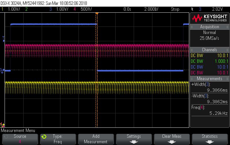
These three pictures are all of the same thing, just at different timebases.
Blue - LED output toggled in data-ready ISR
Red - ADC input pin corresponding to slot 1 in the sequence
Yellow - ADC input pin corresponding to slot 11 (last) in the sequence
I did my trick of putting a 1M pull-up on the two analog input pins, but they’re otherwise undriven. That way you can easily see when they get selected for sampling… the voltage drops like a brick.
In this one you can see the interrupts are coming in at a leisurely 9.4 msecs and that the sampling rate on a given channel is a respectable 5.3 kHz:
This next one zooms in to show that time between the sample-start of the last slot (Yellow) and the sample-start of the following first-slot (Red) is 17 usecs:
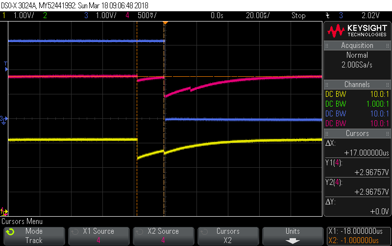
And finally, the third one zooms in even further again to show that the interrupt latency after the sample-start of the first slot (which corresponds to the end of sampling of the last slot) is just 520 nsecs, and a good chunk of that will be the call to
HAL_GPIO_TogglePin(LD2_GPIO_Port, LD2_Pin);

To achieve that I did away with the callback routines and toggled it right in the ISR which is found in Src/stm32f3xx_it.c:
/**
* @brief This function handles DMA2 channel1 global interrupt.
*/
void DMA2_Channel1_IRQHandler(void)
{
  /* USER CODE BEGIN DMA2_Channel1_IRQn 0 */

  HAL_GPIO_TogglePin(LD2_GPIO_Port, LD2_Pin);

  /* USER CODE END DMA2_Channel1_IRQn 0 */
@Robert.Wall
I guess the next step is to start up a second ADC and use the same techniques to determine how precisely we can offset their start times, and also ensure they then stay in lock step at that timeshift. Are you still thinking 0.1° is sufficient resolution? So somewhere around 4-6 usecs resolution, depending on line frequency. I’ve not been paying enough attention but what is the approximate phase shift correction (in degrees) you currently need for your collection of VTs and CTs? Always less than say 5° for the worst case combo? Does Voltage need to be advanced or retarded?