STM32 Development

That’s impossible. How can it know the difference between a failure and a deliberate change? If a sensor dies, then a week later a new one appears, was it necessarily a replacement?

Thank you for the input on the ds18b20 temperature sensing, sounds like studying @Robert.Wall’s example is good first step. I think Il come back this it at a more detailed level later on, I’m happy that I have got the basic example running which is enough to progress to the next step on hardware design.

I have uploaded some of my recent development notes here STM32/stm32notes.md at master · openenergymonitor/STM32 · GitHub and a fourth design variant. It’s a work in progress, I’m trying to go through the main components of a basic design, document the design decisions and get it as clear as I can in my head how it all fits together.

Well it would be a replacement because I would have replaced it. And if I hadn’t done any additions or replacements then no response would mean that the sensor wasn’t well. I’ve never had one fail, so I don’t know how a failure happens, do they go intermittent or just drop off the face of the earth and never come back?

These systems are managed systems, not like say an open wifi access point which doesn’t know anything about what might be accessing it. We set up the systems with the sensors we need to do a specific job, in my case monitoring the Heat Bank temperatures. I have added sensors in the past but I did that, they didn’t appear out of thin air. So I knew what was going on and could then link the inputs to feeds and then to dashboards.

So IMO it would be very easy to set up and manage the connected sensors automatically.

Simon

That was exactly my point, you know that you’re replaced the old one with one that has a different serial number, therefore you assume it must, and want it to, take the same place in the list of data that’s sent to emonCMS. (Because that’s the pertinent point here.)

Precisely, managed by you. [My emphasis]

If the sketch can always assume that a sensor that has gone missing has gone forever, and the first new sensor it sees is a replacement for that, then yes, it’s easy to manage that situation. But what if you’ve added a sensor, and in the process disturbed an existing one and cause it to fail? What if two have failed and you replaced both, at the same time? You’ll end up doing quite a bit of head-scratching until you’ve found, buried somewhere in ‘Resources’, the algorithm that describes what the sketch has done.

Anyway, this has gone off-topic.

Agree but still worth working through sometime.

Simon

As mentioned above, the first step on my STM32 Development plan is:

“Work through STM32 power supply, clock, programming sub circuits, check understanding, component sourcing. Put together base board design (equivalent of a STM blue pill, or Ken’s ARMIGO) potentially with a couple of CT and ACAC sensor inputs for initial testing.”

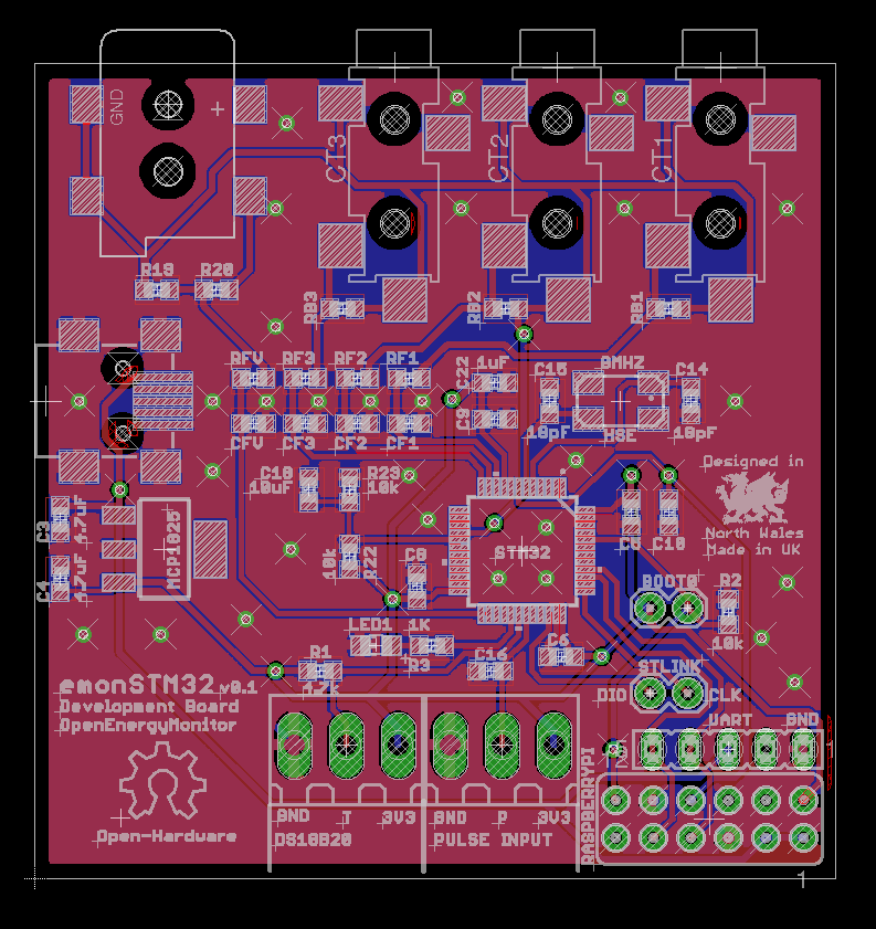
I’ve now put together this first design and will be sending it off to ragworm hopefully tomorrow. I’m fully expecting this prototype to have errors as it’s my first design with this chip. If anyone can spot any, please let me know :slight_smile:

Bearing in mind that the intention of this design is just to test the basics and not to fulfil the longer term project goal of a more capable multi-CT unit, here is the spec:

  • STM32F303CBT6 core 120 kBytes flash, 40kBytes SRAM, LQFP 48
  • 3x CT inputs (ADC1), 1x ACAC input (ADC4).
  • Simple RC filter on each input
  • DS18B20 input
  • Pulse Counting input
  • External high speed clock (8MHz)
  • RaspberryPi hat/shield design to fit in emonbase case
  • OTA RaspberryPi update hardware support
  • On board LED indicator

Design notes:
https://github.com/openenergymonitor/STM32/blob/master/docs/stm32notes.md

Eagle, schematic, board and gerbers
https://github.com/openenergymonitor/STM32/tree/master/Hardware/5

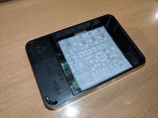
What it should look like in the emonbase/rpi case:

426079805776864060

This is one of those rushing out the door haven’t got time to think it through time comments, so take it with a grain of salt and if you’ve already considered it disregard.

I wonder if it’s worth building some sort of LPF into the op-amp mid-rail configuration to ensure it’s as clean as possible. Others here (@calypso_rae?) have a lot more experience building shared low-impedance mid-rails than I do, so you might want to compare your mid-rail design with theirs. I’m pretty sure stm run all the op-amp pins to the outside world, so you should be able to do anything that you could do with a discreet op-amp.

Thanks @dBC, at the moment I have a 10uF capacitor across the bias voltage divider on the input to the buffer. When I experimented here with the oscilloscope it didn’t make much difference. The bias did seem very stable, e.g no visible indication of interference from the ACAC Voltage adapter. Happy for input on how to improve and I will search for other’s work on this as you suggest.

Thanks for the quick comment.

Here’s the schematic for easier access to what’s in the design so far:

No problem. You might want to consider over/under voltage protection for the ADC inputs for the case where the AC swing exceeds Vcc/2 (high current fault condition in the mains circuit being monitored).

And I notice the “bypass cap” (C1 in the original OEM design current sensor interface) is gone. Was that a deliberate decision, or did it get left off? I don’t really have a feel for whether it’s required in this configuration or not, but others might know.

Thanks @dBC. Yes good point I will add voltage protection in to later designs. We do have that on the emontx v3 and emonpi. I need to do more reading on bias configuration. C1 is the 10uF capacitor I mentioned above, dont think its needed now as the buffer provides a low impedance source for the bias.

Cool. I was just playing around in the GUI with your selected CPU to double-check your pinout selection and it all looks good.

With regards the UARTs I notice you’re running the same UART signals to the RPi header as you are to the ST-LINK header. It might be useful to use all 3 UARTs, 1 for the OneWire stuff, one for energy reports to the RPi and one for debug printfs. I had a stab at adding that to your pinouts and it seems to work (see below). Which UART does the bootloader use for your fancy RPi programming stuff? Hopefully USART2?

Also I’m not sure about the 5V on the UART/ST-LINK header. Isn’t this all 3.3V? What do you plan plugging into that dual plug? I was assuming a snapped-off ST-LINK V2-1 programmer?

Thanks @dBC. Yes USART2 (PB4 & PB3), is there a reason it would not work on the others? I tried I UART1 and UART2 both worked ok.

I noted your comment on multiple USART’s before, it’s great having so many USART possibilities. I think I will explore that further on the next iteration.

The 5V on the 5 pin UART header goes to the voltage regulator, I guess its just an option to power the board from a USB to UART cable… 5V is also routed from the RPI headers through the 3.3V voltage regulator for board power rather than using the 3.3V RPI supply.

The plan is to be able to program with both the snapped off ST-LINK using the CLK and DIO pins (plus supply pins) and a standard USB to UART in the 5-pin header below.

Do you see any issue with the flash and sram size for the STM32F303CB? My back of the envelope calculation suggested 23.4 kBytes of SRAM use for the DMA arrays (2x 6000 entry long array’s of 2 byte unsigned integers). I’m assuming the rest of the memory use is relatively small.

Do I also understand correctly that a STM32 chip bought from say farnell will be ready for firmware upload with ST-LINK? Reading this suggests that that is the case: stm32 - Bootloader on STM32F303: built in from factory or externally programmed? - Stack Overflow

Actually, you’ve taken the lead on that aspect. I’ve only ever programmed these things via the ST-LINK. When you reported success on RPi programming a while back I assumed (obviously incorrectly) that the bootloader must have a hardcoded UART that it waits for an image to arrive on, but perhaps it monitors them all and uses whichever one starts talking?

If it does get tight you can always reduce those array sizes, they’re pretty arbitrary. I probably went large in the example code because we were running on a device that had heaps of RAM. Assuming a given sampling rate, the array size simply determines the interrupt frequency. If you were to halve their size say, then the interrupts would occur twice as often, but you’d have half as much work to do on each interrupt. If you were to make them ridiculously small then the ISR overhead might start to become a significant part of the load which wouldn’t be good, but I think we’re a long way from that happening.

Yes, exactly right. I think of those CLK and DIO lines as stm’s version of jtag… very low level and let you flash your image pretty much regardless of the current state of the device. Just make sure any image you build/flash also has those pins enabled: Sys->Debug->SerialWire in the panel on the left (see screenshot below). If the two pins are showing up as Green then you’re good to go.

I don’t know whether that’s the case for the serial programming technique you’ve discovered because I’ve never used it.

1 Like

Thanks for all the input @dBC much appreciated. Thanks for the pointers on the arrays and enabling the CLK and DIO lines. I will press go on the PCB order and feedback on testing once they arrive :slight_smile:

But wait! ;-).

I think you need NRST on that STLINK header too. Which signals did you hook up when you did your snapped-off-STLINK programming experiment a while back?

We run 8 signals to our programming header:

VCC, GND, NRST, SWCLK, SWD, SWDIO, STLINK_RX, STLINK_TX

I think VCC is so the programmer knows what voltage the target is running at. SWD I don’t use but I think it permits trace/debug stuff.

Here you go… you had five wires hooked up: https://community.openenergymonitor.org/t/stm32-hardware-development/7135/20?u=dbc

:slight_smile: Good spot. I had a mental note in my head that I was getting around that by setting BOOT0 manually with a jumper, powering off and on the board and then its ready for STLINK upload. Double checked it now and it does work. But I’m not actually sure why I didn’t include a pin for NRST as that would of course be easier… I do have it routed to a pin on the RPI header so I can always test with that.

Yes, I guess if you’re using individual flying leads and pins it doesn’t matter too much. I think you do need to run Vcc as well (3.3V definitely NOT 5V) so that the programmer can see the target is powered (and see what voltage it runs at). I’m still a bit nervous about having 5V anywhere near that header… but so long as everyone knows what they’re doing it should be ok.

Thanks @dBC, I’ve modified the board to include NRST and routed 3.3V to the UART header for easy access. I’ve put the 3.3v line through a jumper as the UART 3.3v will otherwise potentially conflict with the 3.3v on the board from the VREG, not sure if that’s an issue or not.

I also realise I had left in a 3.3v track to the RPI header which was not needed :slight_smile: now removed.

It shouldn’t be necessary, but I remember one user who did this found the op.amp. was taking off and oscillating, so don’t take anything for granted! You may well find a much smaller value or even a Zobel network might be needed - it all depends on what the centre rail looks like as a load on the op.amp.

1 Like

Thanks @Robert.Wall I will keep an eye on it. I though I had better include it on the design just in case.

Using the forum search tool uncovers Learn | OpenEnergyMonitor which you of course added :slight_smile: and I’ve been reading through some of the older threads too.