But after switching off the load, voltages get back to normal.
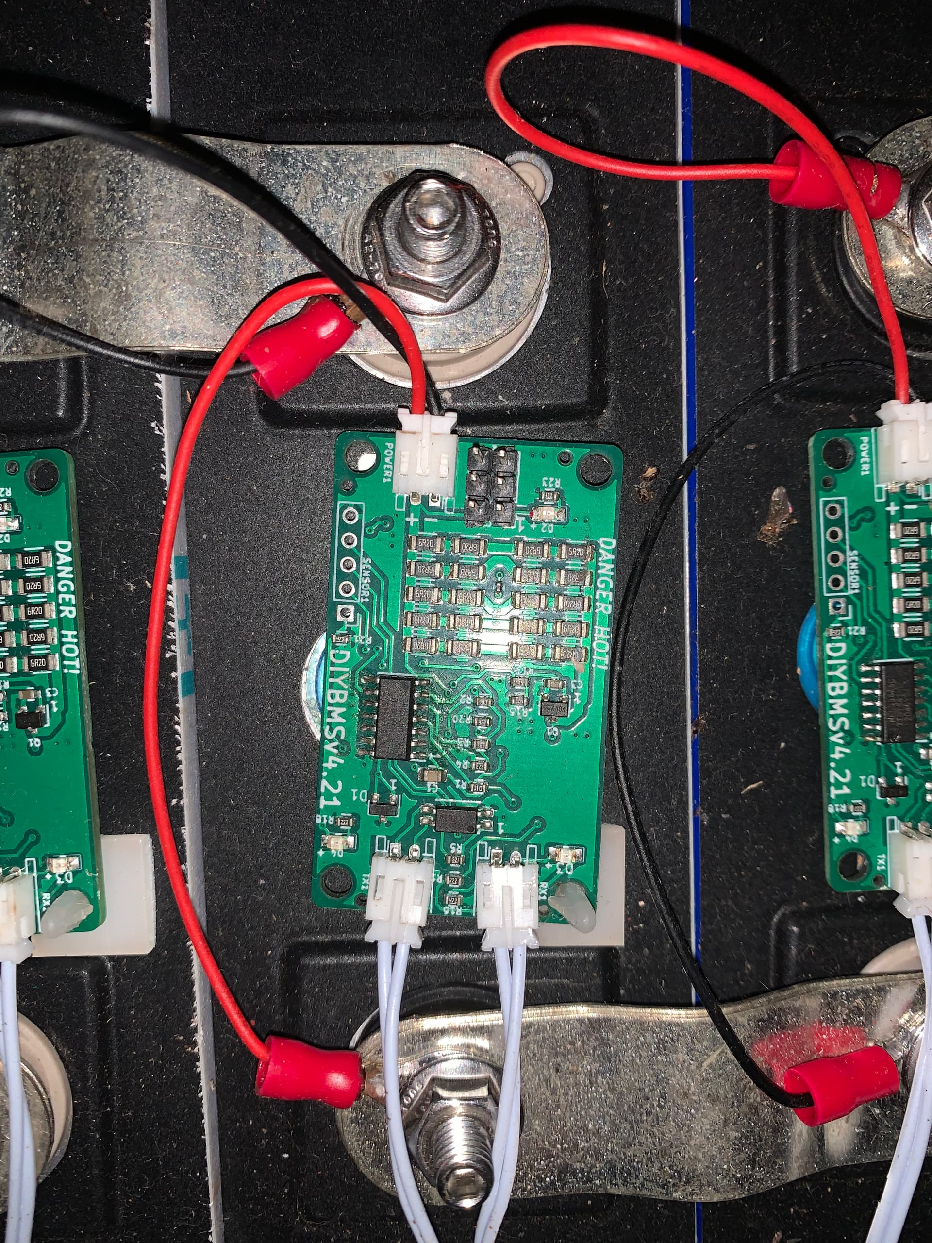
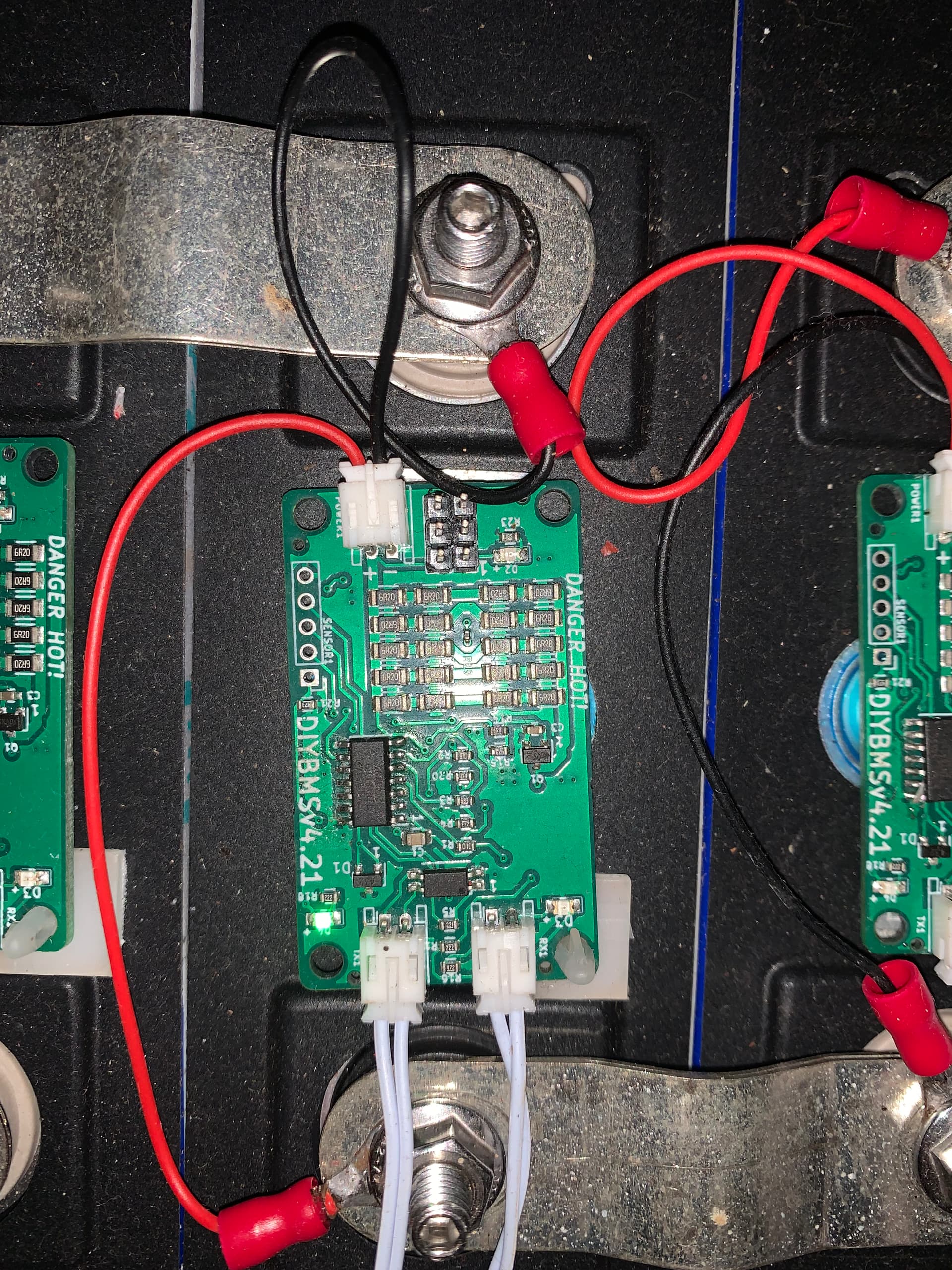
I have 4.21 cell modules (16 pcs) and esp32 controller board (early version with two sets of TX RX).
Any Idea how to fix this?
Hi Stuart,
Thank you for the reply,
Modules connected to cells with copper lugs. Wires are soldered to the lugs. Other ends of the wires connected to JST connector.
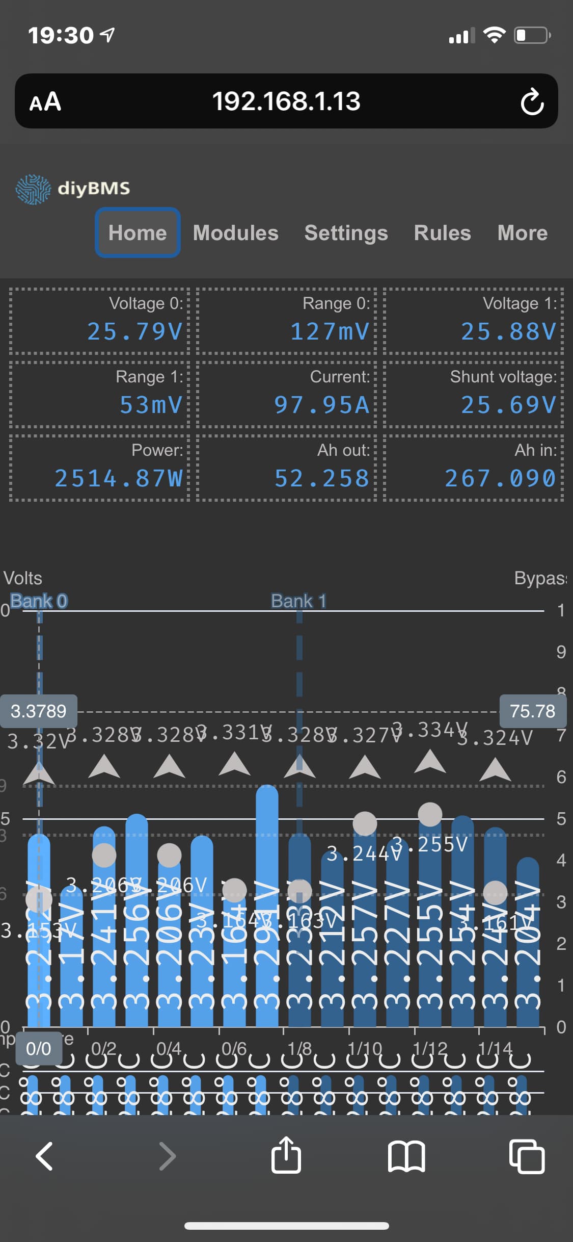
Tested with multimeter and on a load nearly 75A, voltages of all the cells drop to a certain level but stay stable at that level.
And yes I have a EASun iSolar SMV III 3KW model hybrid inverter on this battery pack.
Controller board is powered by the battery pack through a DC step down power supply.
I think the problem is due to cell voltage is not measured for all cells at the exact same time and the cell voltage is measured over a very short time (microseconds). A inverter is switching and drawing not the exact current constantly, if you look at the signal on your DC coming from the battery with a oscilloscope you should see a amount of noise. I expect the difference in measurements of the modules are all within the voltagePeakPeak of this noise.
@stuart can you clarify if the modules are doing single shot measurements or multiple measurements in a short time and calculate the average? If it is multiple measurements without average this might be the reason for floating voltages during discharg and charge that is introduced noise on the DC
@stuart if IT is single sample than i would charge the code to for example 5 samples in 10ms and calculate the average my expectation is that will solve the floating voltage issue.
i have the same problem but only when charging at 20Ah, 100Ah draw is ok.
the voltage deviation increases but stops as soon as i stop charging.
Multimeter shows a stable voltage.
Shorter communication cables and rerouting seems to help a lot,
i used to loose communication immediatly now only 50mv difference.
Don’t ground shielded cables to a noisy ground.
You may have a com cable too close to a power cable.
Try a powerbank or ac adaptor to see if the stepdown is making noise.
Thanks for the photos - I ask because I’ve seen boards with a missing “D1” component - the board works fine, but the voltage readings are all over the place.
I think as @Albert mentions a sampling average of the voltage would smooth the bumps and lumps of the voltage - this is bouncing around when the inverter is pulling energy from the cells.
The downside of this, is the increased duration of voltage readings would make the data transfer through the modules slower - not ideal.
I’m happy to put code together to look at this issue, if you would raise me a ticket on GITHUB -
I’ve also implemented a 5 sample reading for the voltage, if you try this firmware for the V4.21 modules (it only works on that module version for now)
Sorry for the delayed reply. Still in office and couldn’t get a chance to reply.
I’ll try this and let you know the result.
Thank you very much for spending your valuable time and sharing your knowledge!
I’ve been meaning to ping you for sometime about this topic.
Over the last few weeks I’ve been looking at the module circuits and the code - but for now lets focus on 4.4 as that is what i have.
I’m on the road without tools and my notes so sorry this will be terse - sorry and without testing which is what i wanted to do first - but with this topic hot i thought it was best to ask if i have the bull by the horns…
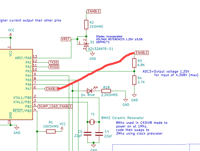
But to me (with my very little experience) I find it surprising that you can get an accurate cell voltage reading when the voltage you are reading is not from the cell rather it is the output of a pin of at the attiny841.
While the pin will reflect the raw voltage it is much more likely to be affected by incoming serial data and other electrical noise.
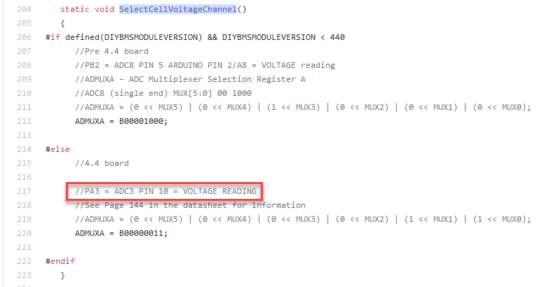
Looking at the purpose of PA7 (enable) it appears you are trying to reduce the standby current of the modules by turning on and off the reference voltage D1 but you are also turning on and off the quasi raw Vcc cell voltage.
Could it be you meant the top of R3 to actually be connected to Vcc where it gets a real raw reading and not switched by PA7 (enable) ?
If this is the case then it is a simple mod on existing bard to cut the trace and bridge R3 to Vcc.
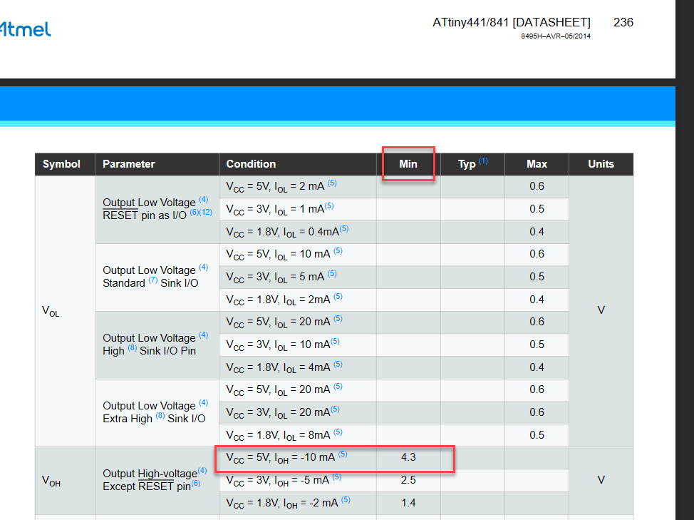
Furthermore if we look at the atmel datasheet the output of pin isn’t true Vcc but typically slightly under.
Another possibility - is (part of) the problem noise on Aref by virtue of the un-bypassed zener diode D1? I appreciate that bypassing it will necessitate a delay in reading the voltage while it stabilises, and it will cost a little in energy as the charge on the capacitor is largely wasted.
I think averaging the voltage reading will also help during charging as most chargers also introduce noise on the cell voltage. In bad cases it might kick in bypass and switch of the charger based on peaks in the noise.
I see some people write " on my multimeter voltage is stable", that is correct as a millimeter needs time to measure see this Link for some information on how much time a multimeter needs to measure and display voltage values
The output of the pin is actually quite stable, there isn’t any serial data comms going on when we take voltage readings (given the way the packets of data flow between modules) and the ATTINY is put into deep sleep to reduce noise when the sampling occurs.
If you connect the R3 to the VCC rail, it will be always “on” and using a small amount of current through the voltage divider resistors - obviously these modules need to be as frugal with energy as possible, hence the switching of the input voltage.
From what I see, the voltage is stable on the scope, and the different between true voltage and the pin output is calibrated for in software (to also cater for the voltage divider resistor tolerance)