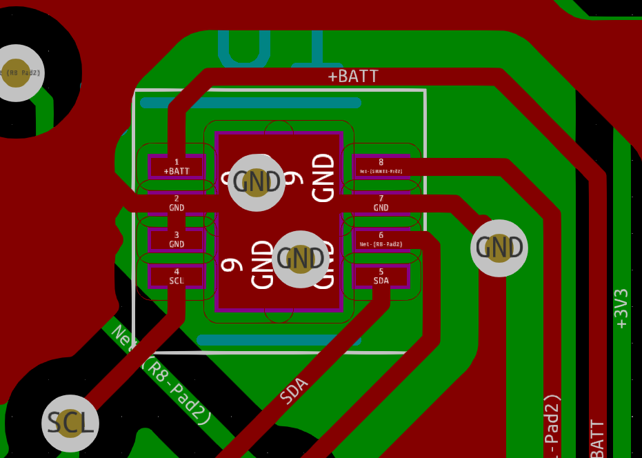
Hi Mike, I think its the rendering from JLC that makes it look a bit close.
Screen grab from KiCad.
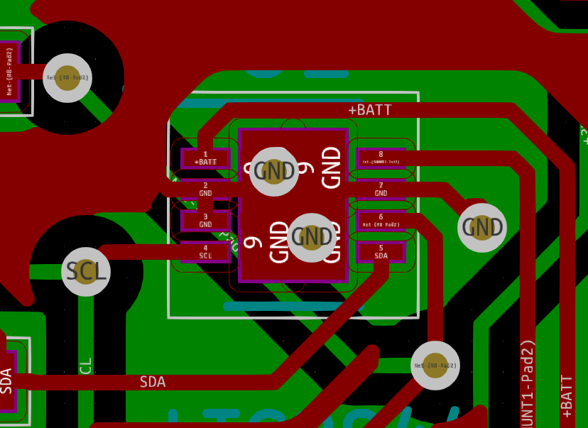
Ahh, yes, it looks like you might be right. I’d likely push the +BATT about 1/2 trace width towards the top away from the GND pads but otherwise it looks good in KiCad rendering.
great! you might also consider similar adjustment on pad 6 and move the GND that is to the right down into the larger fill area
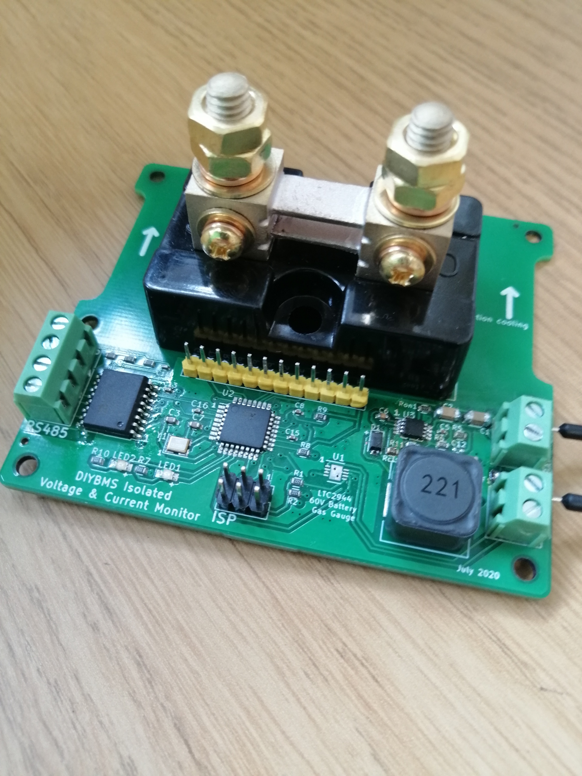
nice was that assembled by jlcpcb ?
Some of it was, most of it by me!
![]()
I have my version of the controller board running with 2 INA226 chips. It seems to work fine.
The INA226 has 2 settings that control how it samples the shunt. It will average samples, which makes sense. It also has a conversion time setting which does not make much sense to me. In theory a longer conversion time will reduce the effect of a noisy reading. Is the ADC essentially averaging on analog side before converting to digital?
When I had these 2 set at the defaults, the amps looked OK with my DC loads. When I turned on the inverter, it jumped around between the dc load and the peak ac. So it seemed to be sampling fast enough to track the sine wave. I changed the settings to the max and the amps did not track the loads fast enough, so I compromised and put a short conversion time and the longest averaging. I have no complaints now, but I don’t really know how accurate it all is.
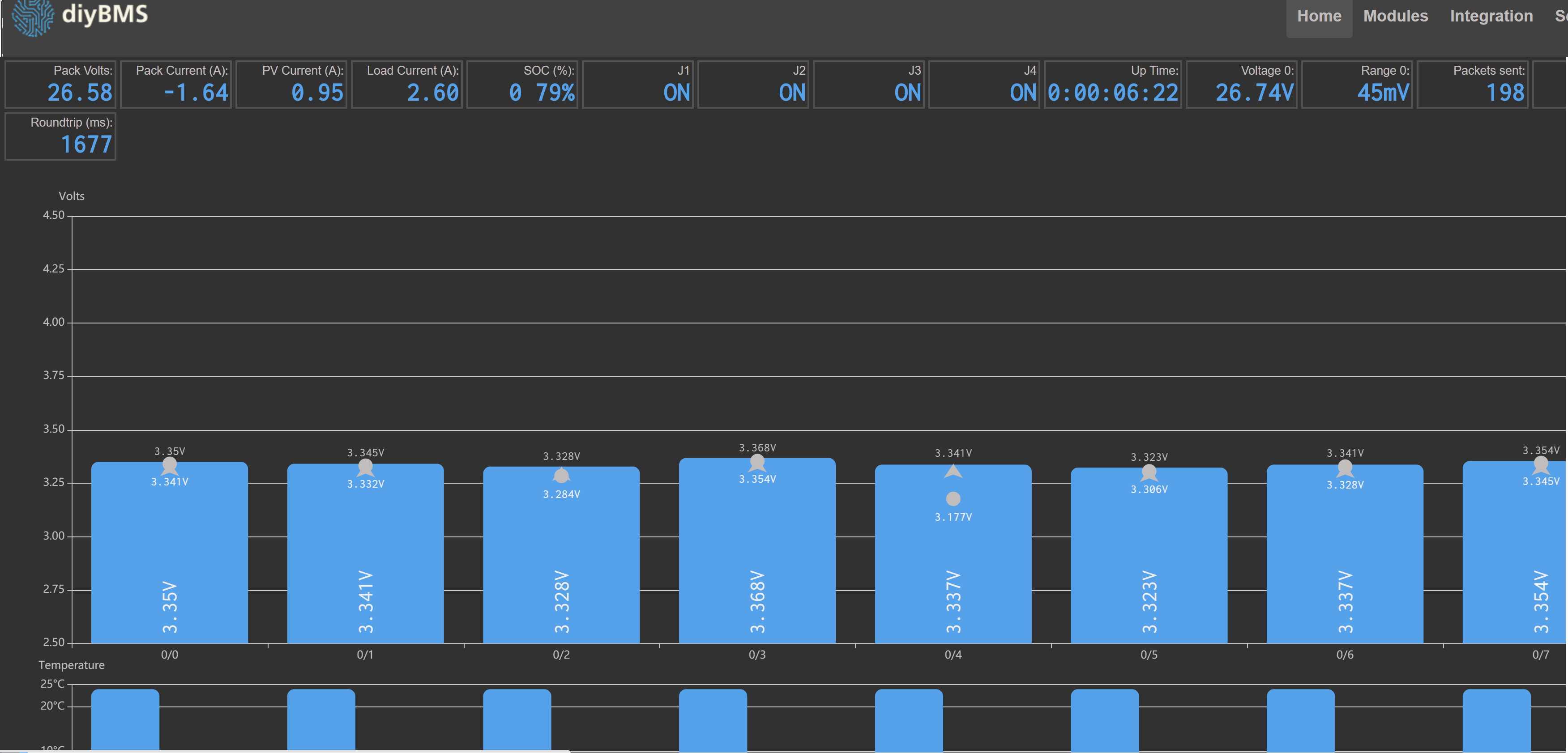
Today, I drove the RV in nice sunshine and it reached my cut off settings of 3.550. My recover setting of 3.400 was respected nicely. The solar was turned on/off properly. When it reached the cut-off, the SOC reset to 100%.
Right now it is night time and the battery is down to 92%, which seems reasonable.
In short, I am a fan of the INA226. I assume the 229 works nicely too and since it is plug compatible, one can use this for a 48v system too.
I don’t see why the design I made is not a viable option for others. I am sure someone with experience could improve the layout. I have no clue about that.
Why not provide others with this choice for the controller?
I’m sure the design is suitable for others with the same requirements as you. I’ve a couple of concerns such as:
Whilst the design works in your mobile RV scenario, this also assumes that the ground of the battery and the controller board are connected together. This isn’t always the case on domestic installations - for instance the user may be running the controller from a USB adapter - using your design now connects the ground/negative of the battery to the negative of the USB adapter output. Is this good or bad? I can’t tell so I don’t want to see users destroying the boards or worse should something “bad” happen.
Whilst the diyBMS is open source, it has my name attached to it. I won’t stop others from modifying it or adapting to their needs, however I need to be careful adopting those changes into the core. Everyone else would then assume it is my work/recommendation on a particular piece of code/design.
If I do adopt something into the core, then there is an expectation on “me” to provide support in the forums and on YouTube/Facebook etc. This is difficult if I didn’t design or have a 100% handle on how something works.
The more variants of the board that exist, increases testing effort and quality control can suffer.
Please don’t take the above as criticism - that’s not my intention - you just have to consider the bigger picture, bad things happen and I never want to have a hand in a device which causes destruction or worse.
I’m happy to review the design and code you have put together, I’m sure we can use most of it in core.
True, and I forgot this. I am using a 24v to USB converter right now, which I assume has the same ground. However, I also plug it into my laptop to program it while it is fully connected. Usually I put the power cord into the laptop, so it should be on battery ground, but it is going through at least 3 power supplies.
I also have powered it from the laptop battery. It all seems to work fine. But in the future I will plug the laptop in before connecting to the esp.
Thanks
True.
What is your goal with this project? I ask, so that I can judge what to attempt to return to the community. I’m happy to not return anything, but figure I should.
Why do you have your name prominent on it? (e.g. Linux does not have “Linus Torvalds” blatantly all over it). Maybe you’d be happier to be less responsible?
Have you put thoughts into how to let it grow without you having to monitor things? I think that the DIYBMS can have multiple variants on the controller, all using the same code. Each for a different application. If I look at my use case it is not too far from being a competitive solution. By that I mean both money and time. The electrodacus bms is comparable in cost, but requires no soldering. However, it has only 4 optoisolated outputs and they are only 50mA. My version has 6 optoisolated outputs ea at .5A. This makes my DIYBMS based solution a pain because you have to solder, but better because you have to do something at least as difficult to handle some loads with the electrodacus. I can imagine someone might want to provide the soldering/programming and support service (and at the same time dealing with the 5x qty thing that JLCPCB forces upon us), for these different verticals. (e.g. Redhat with respect to Linux)
I am totally eager to have you review the board design I created, especially the pcb. I created it in EasyEDA, but I am not sure what to export to look at the PCB.
I took a very quick look at your schematic and I think it looks pretty good. The only thing I’d suggest is a zero ohm R on the address lines on the INA chips.
Why? To be able to change the address easily after production?
Thanks for looking.
Flexibility mostly, but yes you can use it to change addresses on the devices if necessary. I usually do this for most chips that have a GND or VCC pin so that there is flexibility in changing the voltage or address etc. That and adding a pad for an 0603 or 0805 R is virtually free when ordering with PCBA. Even for hand assembly it is pretty cheap (I picked up 5000 0603 zero Ohm R for $11 USD, most R are around this price when ordering by the reel).
One other thing I just spotted on the design, double check the current sinking of the PCF8574T and the TLP222A. It looks like it might be just on the edge of recommended limits for the two devices if all IO outputs of the PCF8574T are LOW (GND).
Good point. I failed to think about all being on. My current build seems to be working with 4 on. This design is being produced right now and I will have to pay attention if I use the additional 2.
I remember wanting a larger resistor just so less power is wasted but had trouble finding the size I wanted that jlcpcb would assemble. I am using the EasyEDA thing and it sucks at sorting stuff by oms, or capacitance or whatever.
I will take your suggestion for future prototypes and instead of getting SMT resistors, I’ll get THT resistors and solder them myself so I can be sure to get the right size.
I will bet there are problems you’ll spot with the PCB. I just use the defaults and auto route. I also attempt to put stuff where it will have the shortest least crossed.
Thanks, the feed back is totally appreciated.
Yeah, I found the same problem for a few components on my designs (one board I’m waiting to arrive has ~140 components of which all but 15 are SMD). I found going with 0805 or 1206 sided components I could find most of them in the “basic” lists. Some though I opted for the larger package size and will hand solder (0805 is not too challenging to solder, 1206 is even easier)
Yeah, keep it in mind and definitely track how much current each relay is actually consuming. With a 560 Ohm R you will be having approximately 3.57mA through the LED. You might need to drop the R down to around 240 Ohm (C23352) which will yield around 8.33mA to the LED.
Definitely don’t blame you one bit! I have a large selection of THT parts on hand for exactly that reason and even more SMD components for projects since they were cheap.
KiCad doesn’t offer auto-routing but I’d use it as a guide for manual routing. I have also customized the settings to work well for JLCPCB (smallest trace is 0.16mm and used only for a few logic IO signals). I also have increased various trace widths to ensure they are sufficient for around 50% over the expected current loads and double up on a few components in parallel (reverse current protection diodes as example).
Shorter traces are generally easier to debug so that is good! In my manual routing I first locate the majority of the components and then evaluate the routing of traces and adjust as needed. I also usually start with the power traces first as they are the largest traces on the PCB in my case (2.6mm for 27V@5A+) and then move to the logic traces. I usually reroute them a few times until I have the fewest vias and odd routing, and then go back in and add multiple vias for connecting the top/bottom GND planes and a few for thermal dissipation.
Without someone being responsible for the project, the project would be a chaos - multiple versions, no one know which one is latest one, compatibility issues and so on (and linux kind of is a chaotic project, imho). So, I fully support the way, Stuart has chosen for DIYBMS: when you use it, you know where it comes from, you know that it is tested and safe to use, you know that there is a way to find some support.
However, your ideas are also good and could be used in some particular cases (If the stars in the sky converge in such a way that someone will have exactly the same setup as yours, well, or very similar). For example in my setup there are 5 PV fields and 4 inverters, should I say now that everyone should have a BMS with 9 shunts only because I wish to see all this loads separately? I do not think so…
But, as mentioned above, it is good to have new ideas and alternative options, maybe some needs exactly the same solution as you use, so it could be shared in a separate/alternative branch. A good example of this - is a LEAF design for cell modules. It is done by someone else, hosted by Stuart. Perfect solution for everyone - if some need an alternative for a specific task - it is available, otherwise - the is a general core that suits most needs for general applications.
I’ve just done the same with the shunt board, I was using some 04 and 06 parts but just swapped back to 0805. Makes routing a little harder for small PCBs but so much easier to fault fix and swap parts.