ST-LINK JTAG/SWD Firmware Upload
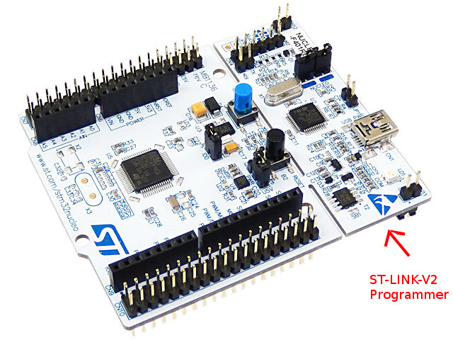
The nucleo development boards come with an integrated ST-Link-v2 programming board that you can snap off.
The ST-LINK/V2 is an in-circuit debugger and programmer for the STM8 and STM32 microcontroller families. The single wire interface module (SWIM) and JTAG/serial wire debugging (SWD) interfaces are used to communicate with any STM8 or STM32 microcontroller located on an application board.
ST-LINK-V2: ST-LINK/V2 - ST-LINK/V2 in-circuit debugger/programmer for STM8 and STM32 - STMicroelectronics

Alternatively you can buy cheap ST-Link-v2 programmers on ebay that avoid the need to add the full st-link programmer hardware to a STM32 hardware design. Ken’s ARMiGO design above has a 5-pin connector for programming with an external ST-LINK programmer.
In order to further my understanding of the hardware part of st-link firmware upload, I snapped off the st-link adapter on my nucleo development board and then following the pin out as documented on the schematic for the nucleo rewired both parts together:
Download the nucleo f303re schematic here:
http://www.st.com/resource/en/schematic_pack/nucleo_64pins_sch.zip
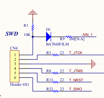
The 6-pin SWD connector can be seen on the left of the ST-link adapter board.

Pins
- n/a
- T_JTCK: Clock signal of target CPU, connects to PA14 on STM32
- GND, connects to GND
- T_JTMS: → SWD data input/output, PA13 on the STM32
- T_NRST: Reset → NRST on the STM32
- T_SWO: Single Wire Output → PB3 (Optional, not needed for firmware upload, used for output)
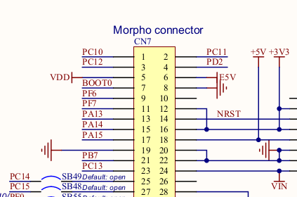
Then on the nucleo development board part, the schematic indicates the position of PA14, PA13, NRST, 3V3 & GND:

3V3 power for the nucleo STM32 board can be accessed from JP1 on the ST-link programmer.
Picture of the connected boards:
and firmware upload worked just the same as pre snapping off the ST-link board ![]()