Problems with emonTx4 + 6 port CT expansion

Hi Forum

I’ve just upgraded my Tx4 to 12 CT ports. It’s a single phase supply to my house. I managed to follow the instructions to build the firmware and install it ok but I have a few problems all of which may have a single cause possibly/probably/hopefully point 1.

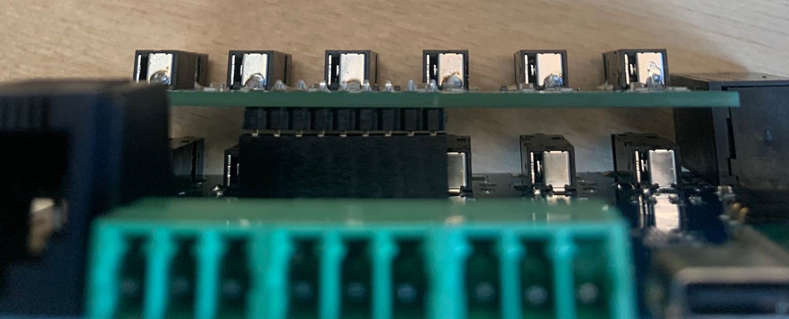
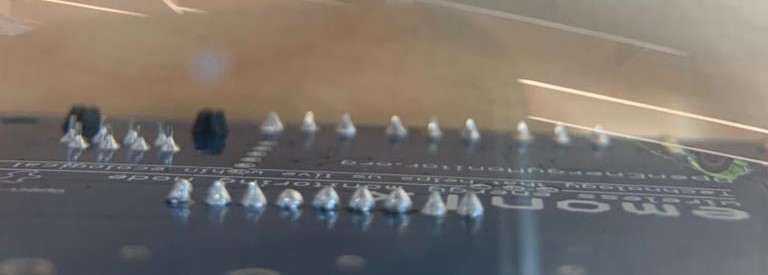
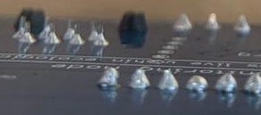
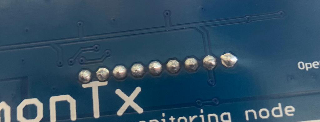
  1. The expansion board won’t sit in the connector properly. The pin for CT12 doesn’t seat as far in as the other pins by a couple of millimeters and so the board wobbles over that proud pin.

  2. I stop getting data from ports 9-12. They work for a few hours and then stop. As an Example here’s one console output:

Ch 1 I=15.778 W=3615 VA=3793 Wh=488 pf=0.9531
Ch 2 I=0.455 W=-3 VA=109 Wh=-1 pf=-0.0390
Ch 3 I=11.200 W=2691 VA=2693 Wh=70 pf=0.9995
Ch 4 I=0.337 W=37 VA=81 Wh=29 pf=0.4521
Ch 5 I=2.462 W=452 VA=592 Wh=218 pf=0.7632
Ch 6 I=0.298 W=15 VA=72 Wh=13 pf=0.2140
Ch 7 I=0.045 W=2 VA=11 Wh=0 pf=0.2098
Ch 8 I=1.244 W=215 VA=299 Wh=116 pf=0.7201
Ch 9 I=nan W=0 VA=0 Wh=-1 pf=0.0000
Ch 10 I=nan W=0 VA=0 Wh=-1 pf=0.0000
Ch 11 I=nan W=0 VA=0 Wh=-8 pf=0.0000
Ch 12 I=nan W=0 VA=0 Wh=-7 pf=0.0000

or snippet…

Ch 9 I=0.000 W=0 VA=0 Wh=-1 pf=0.0000
Ch 10 I=0.000 W=0 VA=0 Wh=-1 pf=0.0000
Ch 11 I=0.000 W=0 VA=0 Wh=-8 pf=0.0000
Ch 12 I=0.000 W=0 VA=0 Wh=-7 pf=0.0000

3 I’ve read the firmware instructions and read the info on calibration but I’m not sure how to calibrate the hardware or the CT sensors. My reading is that with the EmonVs power supply there is no need for voltage calibration required, I can leave the default values in place. I’m not sure if the CT sensors need calibration or not.

Any help much appreciated to diagnose if I have hardware and/or firmware issues and what to do to solve the problem.

I suspect your problem is solely the connector. Either it is faulty manufacture, or is it possible you’ve used too much solder and it’s run into the space where the pin goes?

If it’s any consolation, I’ve now clocked up over 1.2 million message pairs from a 12-input emonTx4, so I think the problem is not in the software. This is with the 3-phase software using emonLibDB, but using only the UK domestic single phase. I can’t speak for the performance of emonLibCM with the emonTx4 and 12 inputs.

Each c.t. gives the same output voltage at its rated current, so it is essential to calibrate each input to suit the c.t. that’s used with it – or vice versa, if you want to read the correct current/power/energy.

Thanks for your feedback,

I will have another look at my soldering. I’ve checked it a number of times and I don’t think I have a short but maybe I do, it’s closer than I’d like in a couple of places. My soldering skills are rubbish.

I’m using the same software as you, emonLibDB. I don’t think you can use anything else for the 12 input version.

As far as calibration I’ve set the config for each input as follows:

  EmonLibDB_set_vInput(1, 100.0, 0.16);  
  
  /* Include the next two lines if you have a 3-phase emonVS */
 
  /* 
  EmonLibDB_set_vInput(2, 100.0, 0.16); 
  EmonLibDB_set_vInput(3, 100.0, 0.16); 
  */
  EmonLibDB_set_cInput(1, 100.0, 0.3);         // 0.3° @ 20 A for 100 A CT
  EmonLibDB_set_cInput(2, 50.0, 0.3);
  EmonLibDB_set_cInput(3, 50.0, 0.3);
  EmonLibDB_set_cInput(4, 20.0, 0.3);
  EmonLibDB_set_cInput(5, 20.0, 0.3);
  EmonLibDB_set_cInput(6, 20.0, 0.3);
  
#ifdef EXPANSION_BOARD

  EmonLibDB_set_cInput(7, 50.0, 0.3);
  EmonLibDB_set_cInput(8, 50.0, 0.3);
  EmonLibDB_set_cInput(9, 50.0, 0.3);
  EmonLibDB_set_cInput(10, 50.0, 0.3);
  EmonLibDB_set_cInput(11, 20.0, 0.3);
  EmonLibDB_set_cInput(12, 20.0, 0.3);
  
#endif

I changed the cInput parameter for the rated current of each CT sensor.

Ouch! Don’t practice on your emonTx4. Get a piece of stripboard and a ‘grab bag’ of components, and practice on that. Also buy a solder sucker or desoldering braid and practice desoldering and removing components too. (I’ve never managed to get on with the braid.)

Desoldering plated-through holes – which the emonTx4 has – is VERY tricky and you’re likely to damage it if you try.

If you decide the problem is the connector and you need to replace it, I wouldn’t even try to desolder a 9-way connector in one piece, it would be much safer to destroy the moulded housing in situ without touching the pcb, and then remove the remnants of the individual sockets one by one.

If the calibration numbers match the c.t’s you’re using for the respective inputs, then you should be close enough for most purposes. You can fine-tweak the numbers if you need to.

Here’s a pic of my board in place. You can see it doesn’t quite sit flush plastic to plastic. Do you know if your’s is the same?

Here’s a pic of my soldering job. I watched any number of how-to video’s before tackling this.

Looks ok to me but I’m certainly no expert. I’ve tested the resistance between the six pins for the CT sensors with my multimeter and they aren’t shorted. Any other testing I could do to check the soldering of the other pins?

Mine is sitting a millimetre plastic to plastic too.

I’m sorry to say your soldering does look a bit iffy. Was you iron hot enough? You can actually do more damage to a modern pcb if you take too long to make the joint because the tip temperature is not high enough to get the lead and the track up to temperature so that the solder flows smoothly and quickly.

It’s hard to know what to tell you to do, other than practice on something it doesn’t matter about. If I was checking that connector, I’d use a soldering iron and solder sucker to remove the excess solder (there’s far too much, it should form a meniscus up the pin like coffee up the side of a mug), and the surface should be smooth and shiny. What makes me think your iron was not hot enough is your joints look dull and pasty, and it looks as if the ball of solder is sitting on and hasn’t flowed around the pad. The 6 pins on the left have got the right amount of solder on.

Here’s a GLCD I soldered up a good few years ago:

It might be worth watching the video just past half-way down this page:
https://learn.sparkfun.com/tutorials/how-to-solder-through-hole-soldering/all

Here’s the direct link:

That fourth pin from the left in your photo looks noticeably shorter. I don’t think you’ve trimmed any of the pins, so the pin might have moved upwards into the plastic body of the connector. That’s why it might not be sitting flush.

As for soldering, I usually do the ground pin last. It’s attached to a bigger bit of metal inside the PCB so takes a while longer to heat up. Enough heat is the trick to get the solder to flow properly.

Good spot I think you are correct.

Roger that I will watch the video, have a bit more practice then remove the solder fix pin 4 and try again for a much neater connection.

I think what I learnt from that and some other videos is that the solder I’ve been using isn’t very good for home use and needs very high temps.

Anyway I de-soldered pin 4 and pushed it back out to the correct length and resoldered.

I also resoldered the pins that seemed to be the worst including the ground which I noticed in the pic didn’t have enough solder to cover the whole pad.

The extension board now sits nicely on the connector with no wobble.

I’ve reconnected everything and three hours later all appears to still be working well. Fingers crossed.

Thanks for your help and input, much appreciated.

1 Like

Would you happen to be using lead-free solder? I avoid this like the plague, it’s the old 60/40 tin/lead for me. It has a lower melting point and if you’re struggling, it might pay to change.

1 Like

Yes indeed. I’ve ordered some 60/40

1 Like

Soldering is always about heat and cleanliness. Most issues are caused by not letting the iron heat up enough and the tip being dirty/contaminated.

image

Compare the solder spread from the back left pins to the front pins. Is hasn’t spread at the bottom onto the PCB in a nice cone. Not quite hot enough or not heating both the PCB and the pin at the same time can cause this.

It is just practice :slight_smile:

Sadly everything worked for about 3.5 hours and now ports 10-12 have stopped working again. They always appeared to have some odd readings anyway

I’ve got my multimeter out again and there is no resistance between any of CT10,CT11,CT12 which I assume is not correct? There is no visible short on the bottom side of the board so I’m guessing it’s either :slight_smile:

  1. Solder hiding under the connector on the top side of the board.
  2. Or the connector is damaged
  3. Or as the traces appear to go to the main AVRDB chip, that is damaged
  4. Or I know nothing and should put down the soldering iron and go back to writing software :slight_smile:

Any thoughts much appreciated.

My next course of action will be to desolder everything and start again

Thanks

It’s much better this time, they are all approximately cone shaped and have spread over the whole pad at the bottom.

1 Like

Time for some logical fault-finding. Do you have the schematics? If not, download them https://github.com/openenergymonitor/emontx4/tree/main/hardware and get the free version of Eagle CAD (it’s quite well hidden, but it’s here Download EAGLE | Free Download | Autodesk - link from Sparkfun).

First, eliminate your c.t’s and the expansion board. The extension on its own, looking between the connector input pins and GND you should see 34 kΩ, and between the input pins and 3.3 V you should see 181 kΩ. With a bare plug in instead of the c.t, you should see nothing (open circuit) between the pads where the burden goes, and the c.t’s resistance itself when it’s plugged in (tens of ohms).

You mean close to zero ohms?

The input pads where you soldered the connector go straight to the input pins of the processor.
What voltage does your multimeter use on the resistance ranges? Provided it doesn’t turn on the protection diodes (which I presume exist but don’t appear to be shown on the data sheet), you should see a very high value.(I see “OL”) If you are seeing 0 Ω or close, there’s a problem

I wouldn’t advise this until you’re certain what the problem is. You could easily cause further damage.

I can’t quite imagine how (1) could be true, the solder just wouldn’t flow that far, this is what the green coating on the p.c.b is for. It’s much more likely you have a whisker of solder on the bottom of the board - have you used a magnifying lens to look? Run your finger nail between the pads.

If your problem is (2), you should see the plastic distorted on one side or the other, or both.

If your meter uses a high voltage for its resistance measurements, (3) is a definite possibility. I won’t say anything about (4).

Schematic downloaded.

On the expansion board itself I see:
GND - > 3.3V = 34kΩ
3.3V → CT7 - CT12 = 54kΩ (All six measure the same)

I wasn’t particularly interested in that, bit it’s close enough: its 180 kΩ and 33 kΩ in series, in parallel 6 times, so 213 / 6 kΩ - 35.5 kΩ.

It doesn’t look as if there’s a problem there, did all the c.t’s look sensible?

If they do, and you have 34 kΩ to ground from each connector pin, we can safely rule out the extension board. I didn’t expect a problem there, it was still worth checking. (I’ve learned over the years never to discount anything without checking first.)

I agree it’s best to eliminate possibilities and it was simple to do.

Thanks for the explanation I wasn’t sure why I had such a radically different number.

That’s harder and very fiddly to do as they are all wired inside my consumer unit and the ends of the cables are high up in the cupboard where I normally have the Tx4. I was also short of time. Will get to it tomorrow.

I was seeing close to 0Ω but only for CT10,CT11 and CT12 and only between themselves. I looked the schematic for the Tx4 board though and noted that the CT9 to CT12 outputs connect to PF inputs on the AVRDB vs PE inputs for the CT1 to 8 outputs. The 660 pages of the AVRDB manual was quite impenetrable but there are some differences that between PE and PF inputs so I hypothesised I was over thinking the problem, the resistance between those pins should be zero and so I should test the board again with my new soldering. I have now plugged everything back in and will check again in the morning but so far it looks a lot better than last time and I’m still getting realistic values from all the sensors after 5 hours. Is it possible there’s not an issue with those 0Ω readings?

I’ve had my magnifying glass out and can’t see any issue. I also tried tried the finger nail trick. My GND pin is a bit ugly on (magnifier + camera + zoom) closer inspection. See below.

No it isn’t it it looks fine.

This sent me into a panic. I can’t find this info in my cheap multimeter manual that I’ve had for 20 years, but I checked other similar meters and I believe it trickles a tiny current into the circuit and then measures the voltage to determine the resistance. So I hope that 3 is not possible.

e.g. On the 0 MΩ to 4 MΩ range, the meter will source a current of around 0.1 μA and then measure the voltage across the load.

I’ll see if everything is working when I wake up.

0.1 µA is well within the rating of any protection diode, so damage is unlikely. But again, it’s something to be aware of; and taken into consideration when buying test gear for use around sensitive semiconductors.

An update that everything is working much better than before. I have readings on all ports all the time for the last two days but I still have a strange problem across ports CT9, CT10, CT11 and CT12

With all 12 sensors I monitor nearly every circuit in the house including the grid and my solar system. The ones that I don’t monitor are currently turned off with the exception of the smoke alarm circuit. When all the circuits are added together I usually have a discrepancy from zero of about 5% or as I’m sitting here now 17W.

CT9 sensor is attached to my second floor sockets final ring circuit
CT10 sensor is attached to my basement sockets final ring circuit.
CT11 sensor is attached to my HA and Lighting system.
CT12 sensor is attached to my basement manifold spur for the devices which control my ASHP.

The base readings on these circuits when all the lights are off with the rings having their usual devices plugged in are:
CT9 ->14W CT10->94W CT11->37W CT12->7W Total 152W

When I turn on all the lights the readings change to:
CT9 ->34W CT10->741W CT11->319W CT12->14W Total 1108W

So all four circuits show an increase in power consumption (I have checked and CT7,CT8 are not affected) and the total has gone up 956W. The discrepancy from zero across all circuits has now gone up to 366W on a total consumption of ~1.4Kw or ~25% When I turn the lights back off, all the readings return to their original values.

Graph from the last hour whilst I have been testing:

I think the pic I posted on my latest soldering shows the pins have clear solder free gaps between them? so I am once again in need of any assistance on debugging the issue.

Thanks
Ben