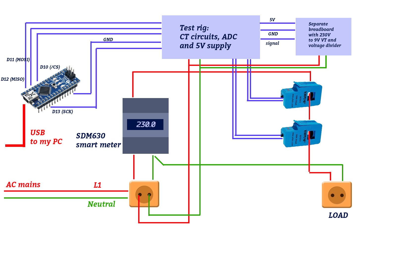
I have another hardware/software problem (actually I think both of them). I have built a test rig with an MCP3208 external ADC and trying to use it to read the CT and AC transformer outputs.
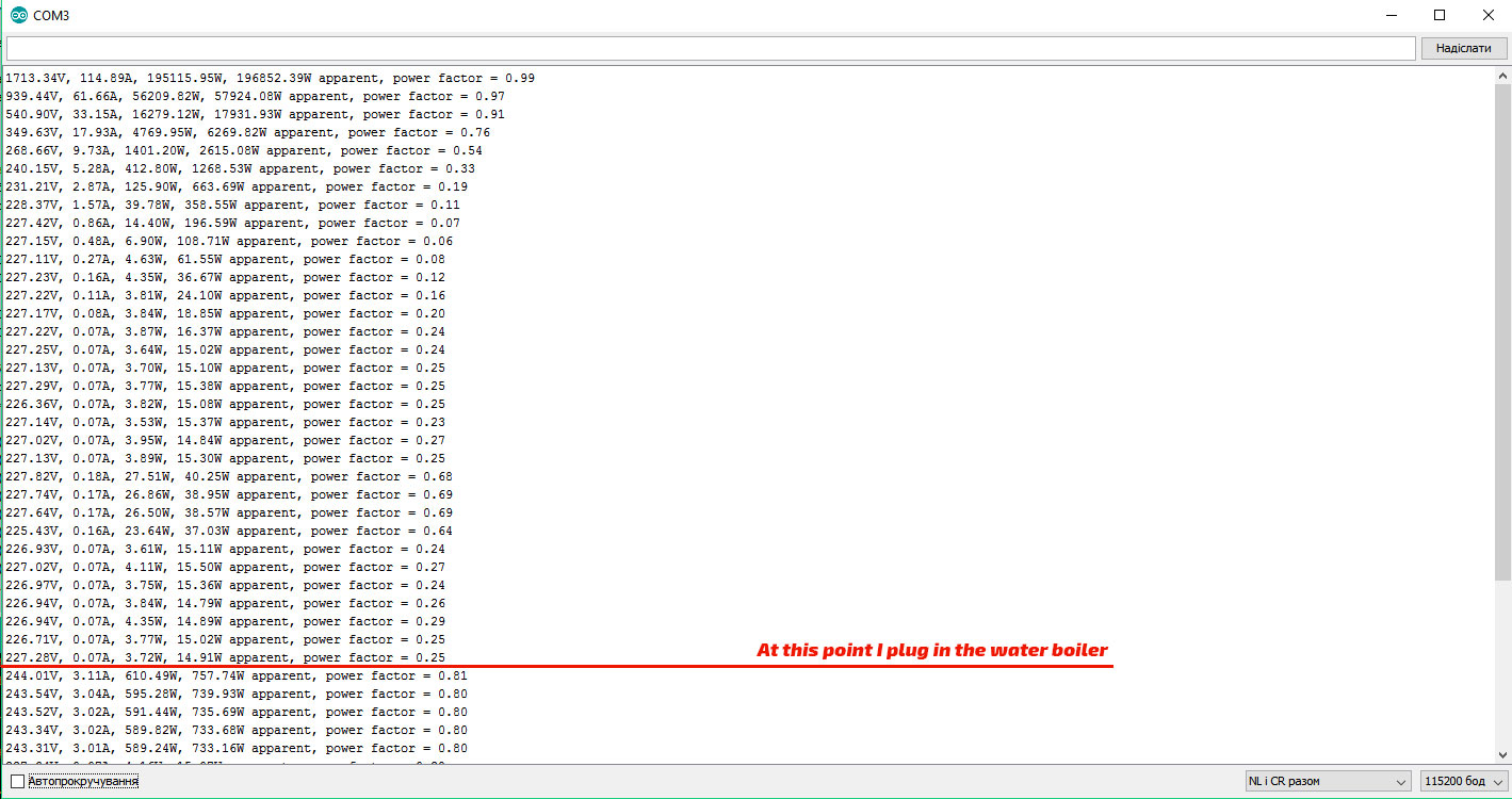
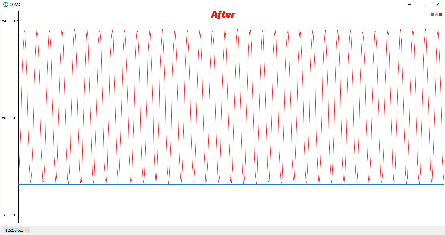
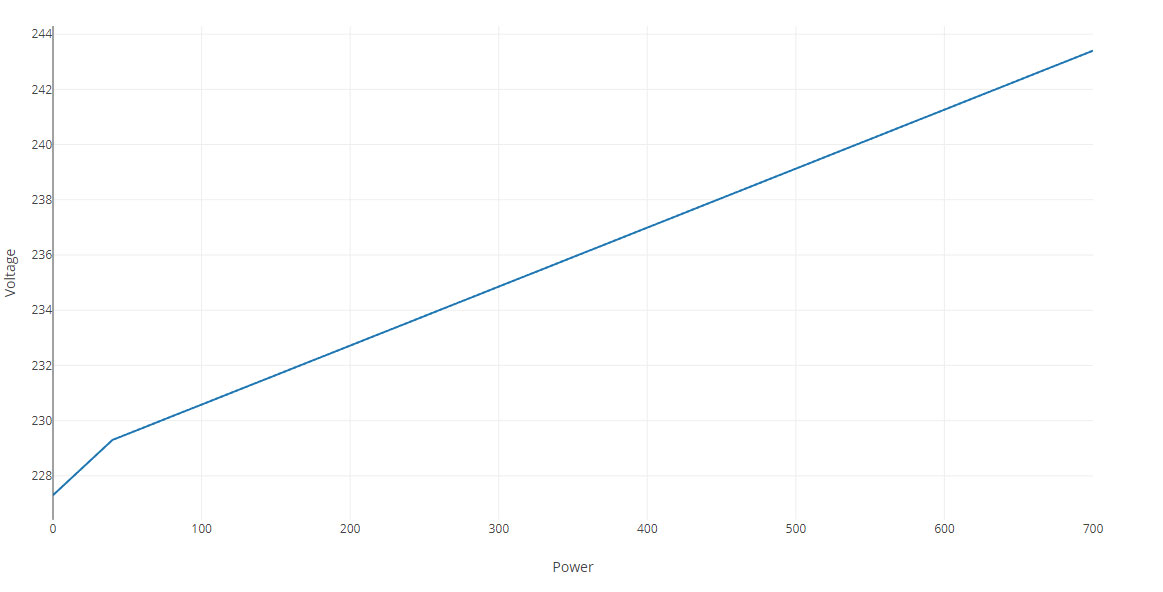
The problem is that when I use the Arduino’s internal ADC with its 10b resolution it’s all good. But MCP shows me a strange behavior: when the rig is loaded with 40W solder iron it shows (almost) normal 227V, but when I plug in a 700W water bolier the voltage increases to 244V
Here are some serial plots and monitor logs from Arduino:
My money would be on cross-talk between your analog inputs, via the ADC’s S/H capacitor. If you look at the datasheet for the MCP3208 you’ll see the SPI clock is also the clock that drives the ADC and that the maximum is specified as 2MHz, and if you do run it that fast you need to ensure your source impedance is low enough to charge the S/H capacitor in 1.5 clocks. Check out Fig 4-2 in the datasheet for more details.
Assuming you’re using a vanilla 5V 16MHz Arduino, then the default SPI clock rate is 4MHz which is way too fast. Try inserting this line after the call to adc.begin():
adc.begin();
SPI.setClockDivider(SPI_CLOCK_DIV32); // Insert this line
Serial.begin(115200);
That will reduce the SPI clock down to 0.5MHz (16 / 32). If that fixes it, or improves it, you can then either calculate your source impedance for both your VT and CT circuits and use Fig 4-2 to work out what speed you can use, or just experiment with the speed.
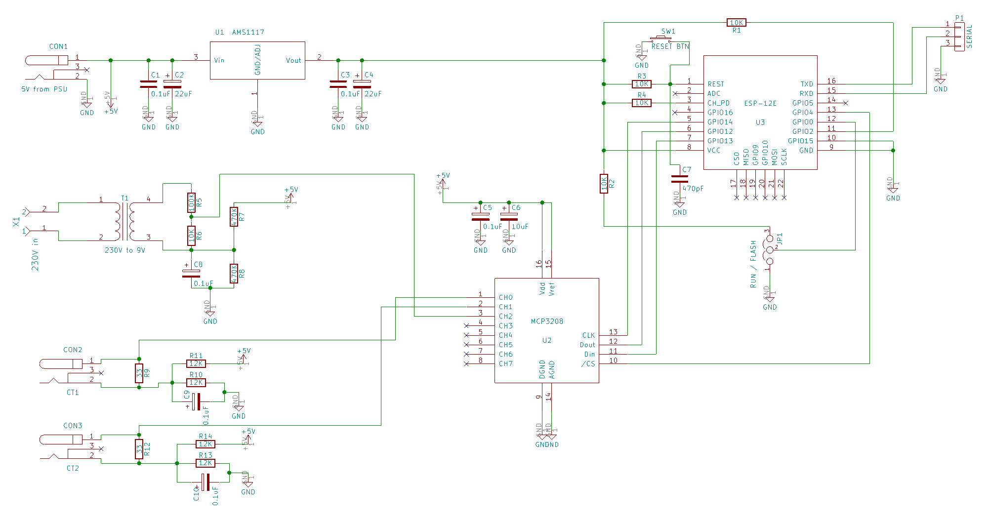
MCP3208 is operating in single-channel mode, CTs are connected to CH0 and CH1 (why there are two of them? Later I want to do some tests on different phases but for now cannot reach any success even on one phase), VT is connected to CH2. All the GND nodes are interconnected i.e. there are no isolated rig parts. Arduino is powered up from USB port. ADC is powered with an external 5V supply (on the PCB with CT circuits).
So there are a lot of unknown here. But there are a few things that don’t add up to me and that the thing works with the Arduino ADCs doesn’t serve to help me dismiss them.
First are the stated facts above. If you have a 9V ac reference, and the VT divider is 100K/10K, that means the AC voltage presented to the ADC should be somewhere around 9 / 11 = 818mv. If you have a 5V Vref (that’s implied but not stated), then your CAL should be someplace around 293.
So I guess I don’t understand why your cal has to be so high. That cal implies that the AC voltage at your ADC is 266mv. Can you measure that? I can’t see doing anything else until that is reconciled. My gut is that it will probably lead to the source of the problem.
Few minutes ago tested the sketch and all the hardware on ESP-12F module (as I planned to test both ESP and Arduino on the same setup). The results are the same: voltage amplitude increases with the load current. So it’s definitelly a setup/wiring problem…
You’re sampling the current and the voltage at best effort time, the time it takes for the cpu to do calculations after each analogRead is dependent on the values of that calculations.
So it could be happening that when a value increases (I) it takes more cpu time to do another while loop and you get slightly different results due to sampling at another position of the sine wave.
Check if the number of crosscount changes with different currents after the same amount of timeout.
That’s not very helpful Robert. The guy is trying to figure out what’s wrong with his experiment and is reaching out to the community. I looked at it and my reaction, somewhat cued by your post that seems to have vanished, was that the numbers were inconsistent and that since it’s in the voltage circuit where he has his problem, maybe he should try to check the voltage with a meter to see if its what it should be.
I referenced your post to credit you with first pointing out the issue.
I’'m not going to get into another hissing contest with you. This is exactly what set me off the last time. Instead of helping us out and pointing out where you think the numbers are wrong, you make demeaning comments. You’re a smart guy and usually get it right, so what did I actually do wrong?
I’m human, I make a lot of mistakes. I learn. This guy is trying to do the same and I’m going to try to help him out.
For the benefit of accuracy, and to be of more help to @dumbassprog (sorry) I’ll be more specific. The cal of 900 on the voltage channel means that 1V at the ADC (everything here is AC RMS unless I say otherwise) indicates 900V at the wall. So when the kettle is on and the sketch indicates 244.01 volts, the voltage at the ADC must be 244.01/900 = 271mv. If it’s not close to that, and closer to 800+, then it’s likely a programming bug that we all missed.
The other calculations were nominal. I didn’t see where the voltage output of the VT was stated, so I assumed it is a 9VAC nominal VT. The actual voltage can and typically does vary, and in all cases I’ve seen, it’s more. Typically several volts more. But the resultant voltage at the ADC will be 1/11th of that.
Current = voltage / resistance.
Current = 9 / 110,000 = 81.8ua
Voltage = current * resistance
voltage across the 10K resistor = .0000818 * 10000 = 818mv
You can measure the actual voltage of your VT and plug it in where the 9 is.
Now, if (when) you have 818mv at the ADC (and you may have more as explained above), and that’s when the wall is at nominal 240, the cal should be
240 / .818 = 293
That’s if the VT is putting out exactly 9v AC RMS when the wall is 240v AC RMS. Your mileage may vary.
That’s a far cry from 900. So I encourage you to figure out why your cal is 3x the expected nominal value.
Is that with the 900 Vcal? Looking at your circuit I think the input impedance on the ADCs is way too high, especially the 470k on the VT circuit. 12K on the CT circuits is in the ballpark (and so is the ICAL) It doesn’t give the sample and hold capacitors enough current to charge. There are a few things that I do differently with MCP3208s to make them work.
When I was using voltage dividers successfully (I use op amps now), I was using 4.7K resistors, with a 10uf capacitor where you have the .1uf cap. I know that works pretty well, but at anything above about 500Khz on the SPI clock, you need to increase the sample and hold time. I developed a technique to do that and I’ll post a link to that later.
I used that circuit on both the VT and CT inputs with success.
The tell tale that the ADCs are not charging to full voltage is that the offset values sag. If you print the offsets out after the thing settles down, they should be around 2048. A much lower value would be consistent with insufficient charging and your need to multiply the result with that large Vcal.
The Arduino ADCs are not as demanding as the MCP3208, but they are also slower. That explains why it works with them.
You should be able to run the ADCs at 1Mhz if you use the S&H lengthening technique. I run them at 2Mhz with the op-amps (very low impedance).
Somehow I missed that at the time, and I’m struggling to get my head around it. If it’s not too much to ask, could you draw a timing diagram of /CS, CLK and DI to indicate your technique please?
The datasheet says:
a sample is acquired on an internal sample/hold capacitor for 1.5 clock cycles starting on the first rising edge of the serial clock once CS has been pulled low.
That strikes me as being independent of what’s happening on DI, i.e. where you’ve managed to position your start bit. But you say:
You can shift the whole transaction left 4 bits so that the S&H period is defined by two cycles that straddle the first and second bytes.
Would that require you to assert /CS right near the end of the transmission of the first byte? A timing diagram sketch of what you’re doing might help me understand, thanks.
[EDIT] - never mind… I read on and saw where it really samples. I assume that datasheet sentence I quoted above is incorrect?
So does your SPI controller let you transfer an arbitrary number of bits? I don’t think the AVR one can. From memory I think it always transfers 8 bits. So unless dumbassprog bit-bangs it all with GPIO pins he may not be able to take advantage of your optimisation.
The short answer is that you can do this with byte oriented SPI. The ESP8266 will do any bitlength, but you can do it using byte boundaries and extracting your result from the result bytes with masks and shifts.
On the leading side of the transaction, there can be any number of zeroes, as the transaction is defined by the start one bit. So three leading zeroes, the start, the diff, then the three bit channel address. That’s the first byte.
Now wait awhile (a really long while with 470K voltage dividers - couple of us with the 4.7K and 10uf cap). CS remains low.
Now read two bytes. The first two bits will be arbitrary bits, followed by the 12 result bits msb first. If you leave CS low and the clock running after that, it will continue with the result in little endian format, beginning with the second bit (lsb is not duplicated). Even after the 11 additional little endian bits are transferred, the data sheet says you can leave CS low and the SPI clock running, and it will continue to pump out zeroes.)
Since publishing that technique, I’ve started using LM358 op-amps for the bias and no longer need to extend the s&h time, but this technique worked great with the 4.7K bias supply and a couple of microseconds extra s&h time. Whenever I would try to reduce it, the sample average (offset) would start to sag from ~2048.
EDIT: I hadn’t looked at that stuff in months and wrote the above from memory. The basic principle is correct but in looking at my code and datasheet, I dropped a bit in the explanation. I’ve corrected that. An entire transaction is 19 bits. When you add the three leading zero bits to byte align the S&H period and transfer 3 bytes, the result is in the low order 6 bits of the first output byte (of the second two byte spi transfer) followed by the high order six bits of the next.
uint16_t result = word((*spiout & 0x3f), *(spiout+1) ) >> 2;