I lashed together an ESP32 with a AC adapter and a couple of CT’s…all works ok so I decided to tidy it up and make my own PCB. At the same time I though I’d use the buffered voltage bias option rather than the simple resistor dividers used in my 1st set-up. I now seem to have run into issues I don’t understand and can’t resolve. The readings are very poor and when I probe between the input pin and the ESP32 ground the signal is awful. Its very noisy and whilst it is 50hz the shape is poor and the amplitude does not follow the current flowing through the CT. Please note I’m testing with a purely resisting (heater) load.
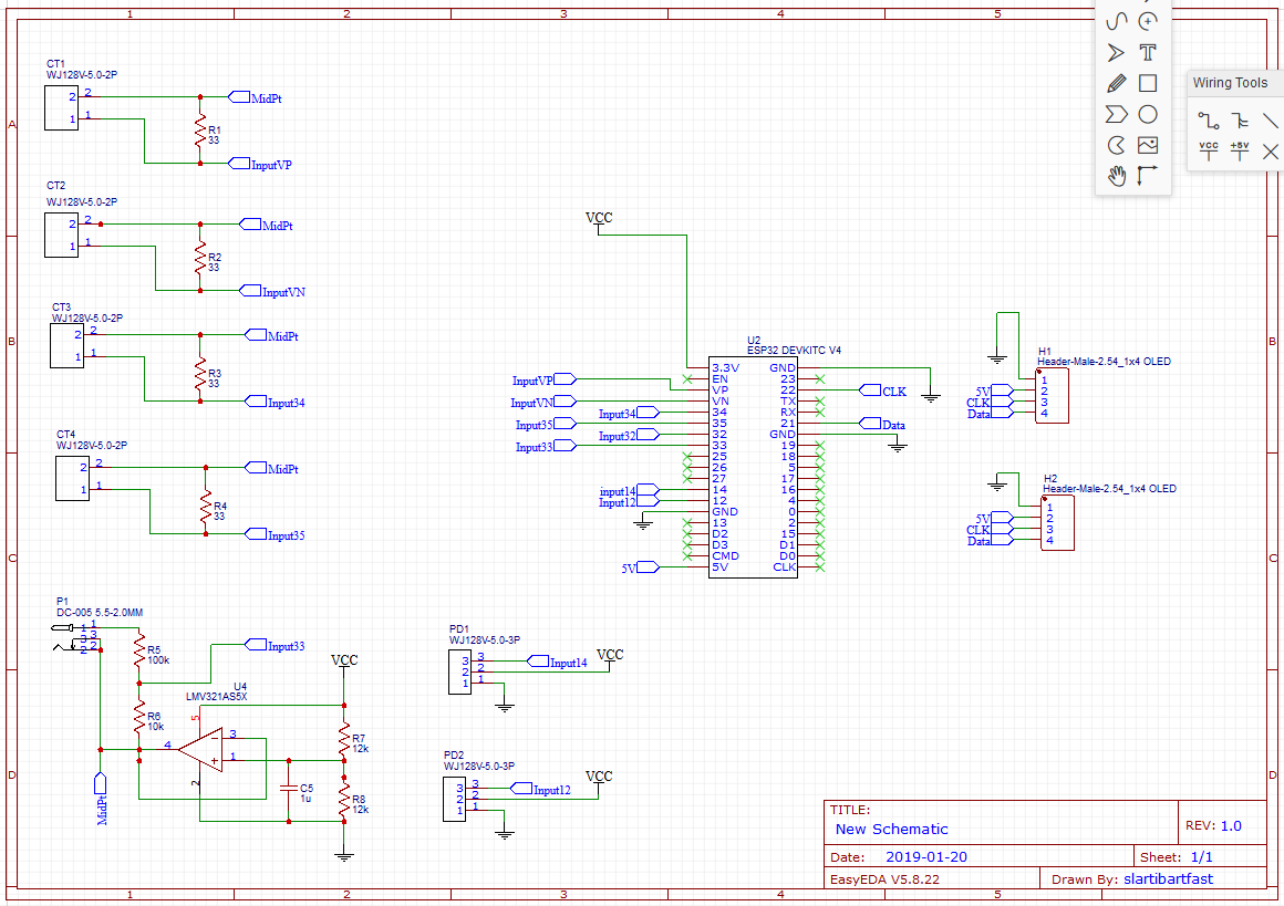
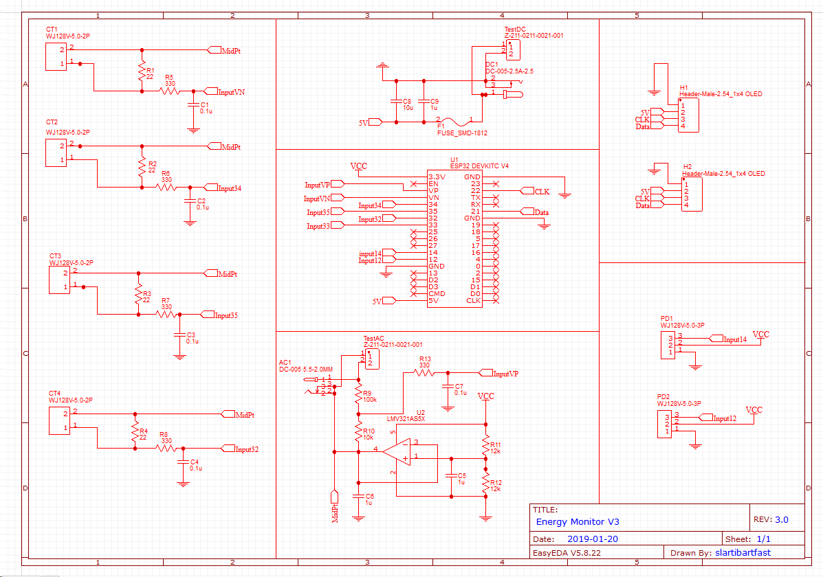
Here is my circuit. I followed the cct diagram from the Learn part of the website and can’t see any differences but I can see that there is a difference in the diagram originally posted by Calypso_rae here. Original post of buffered voltage solution
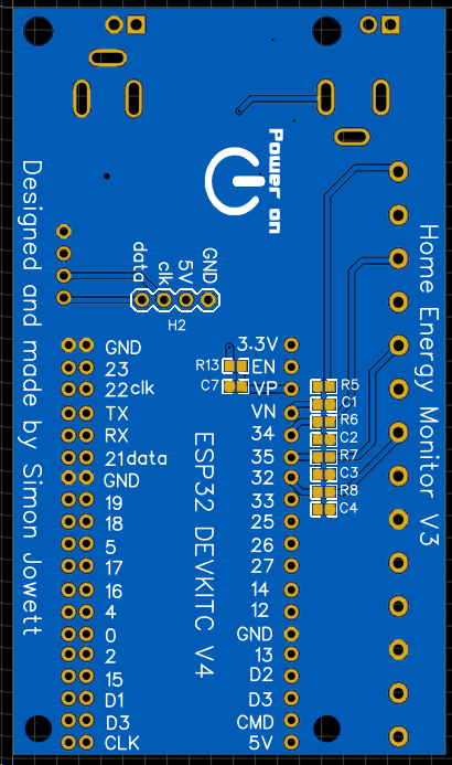
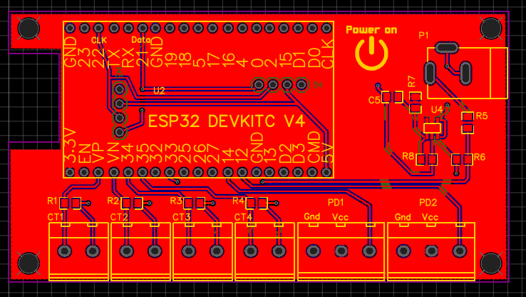
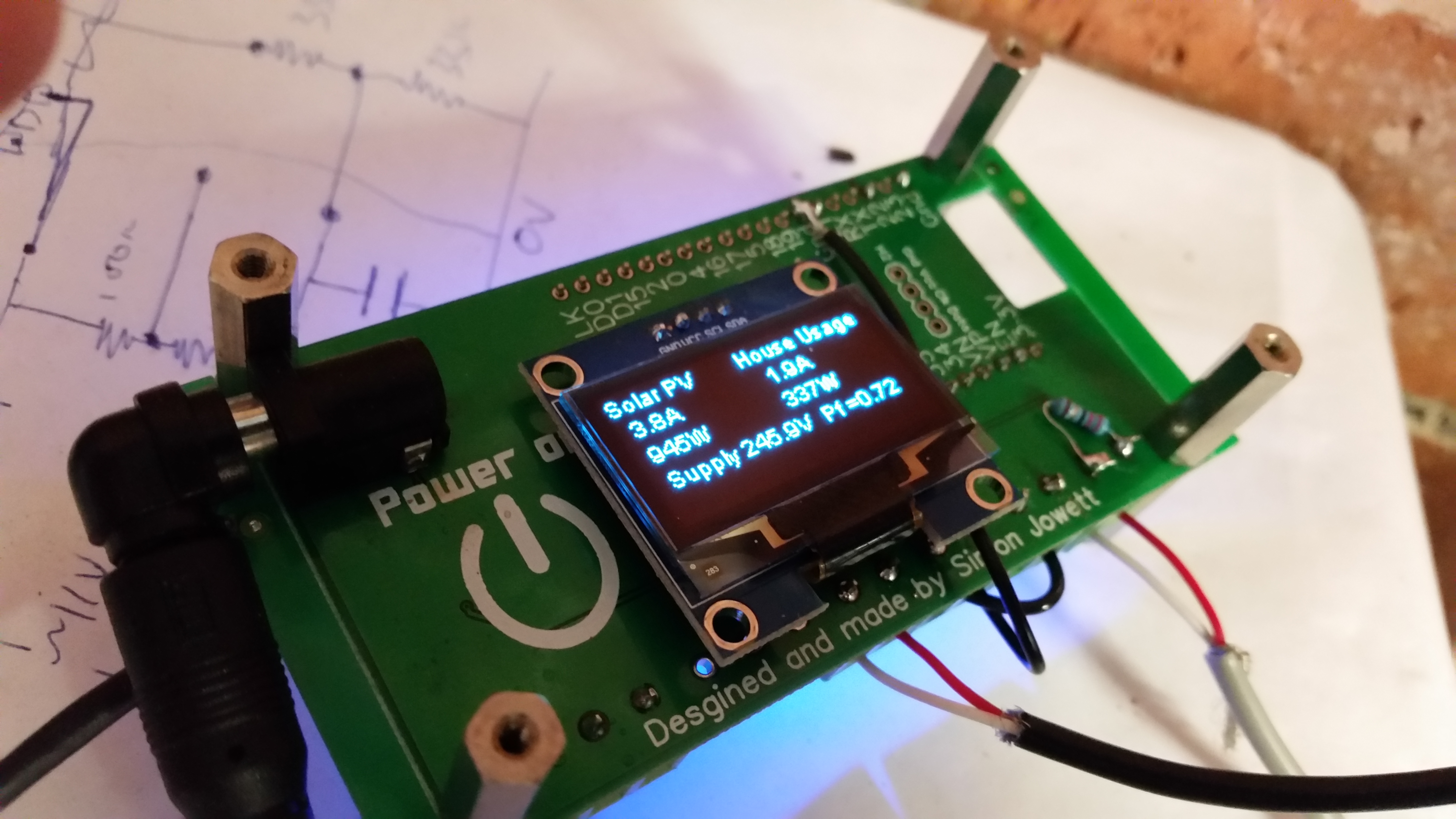
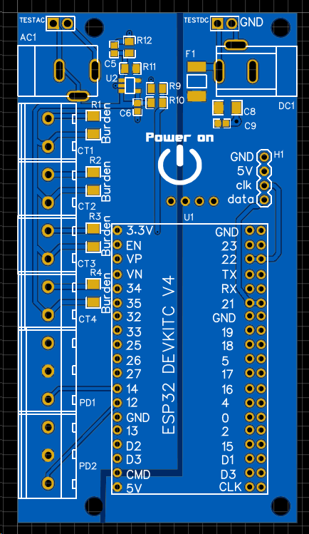
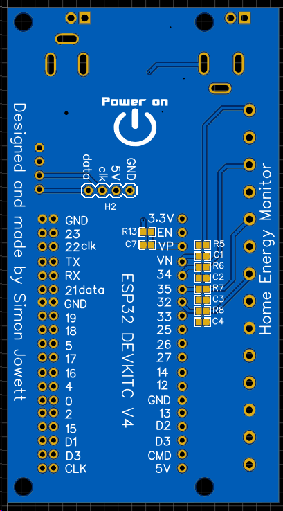
Here is my pcb, the top layer is 3.3v and the bottom is the ESP ground.
My understanding is that the ESP analogue inputs are not very good. I am hoping to try something similar to you but using MCP3202-CI/P A/D converter Channels2 12bit .
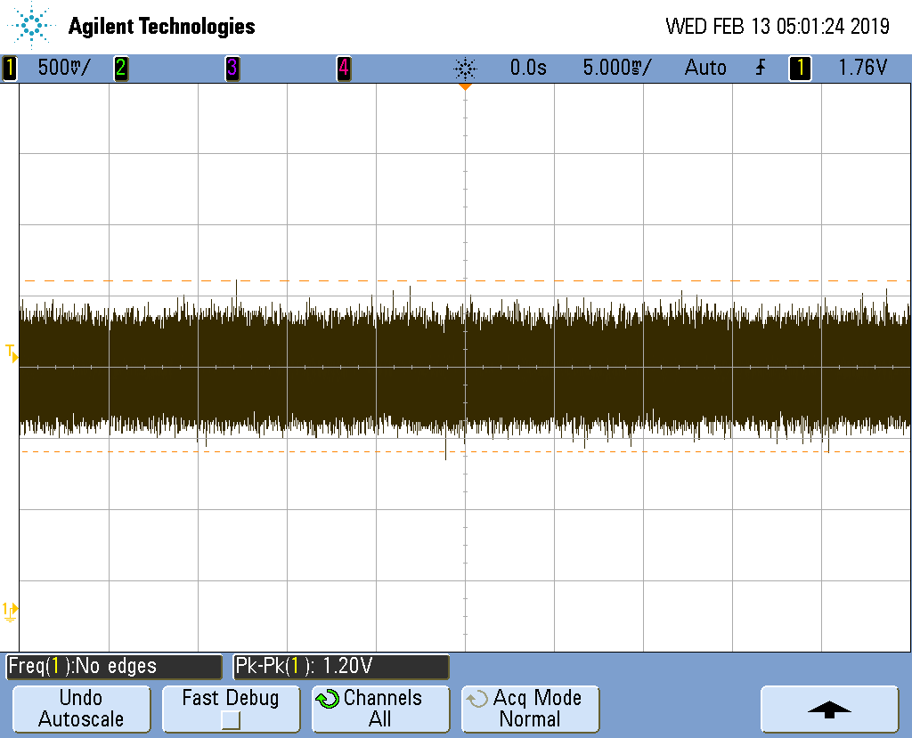
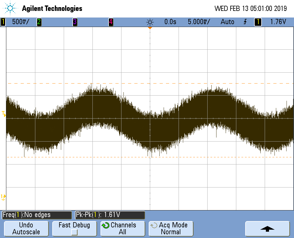
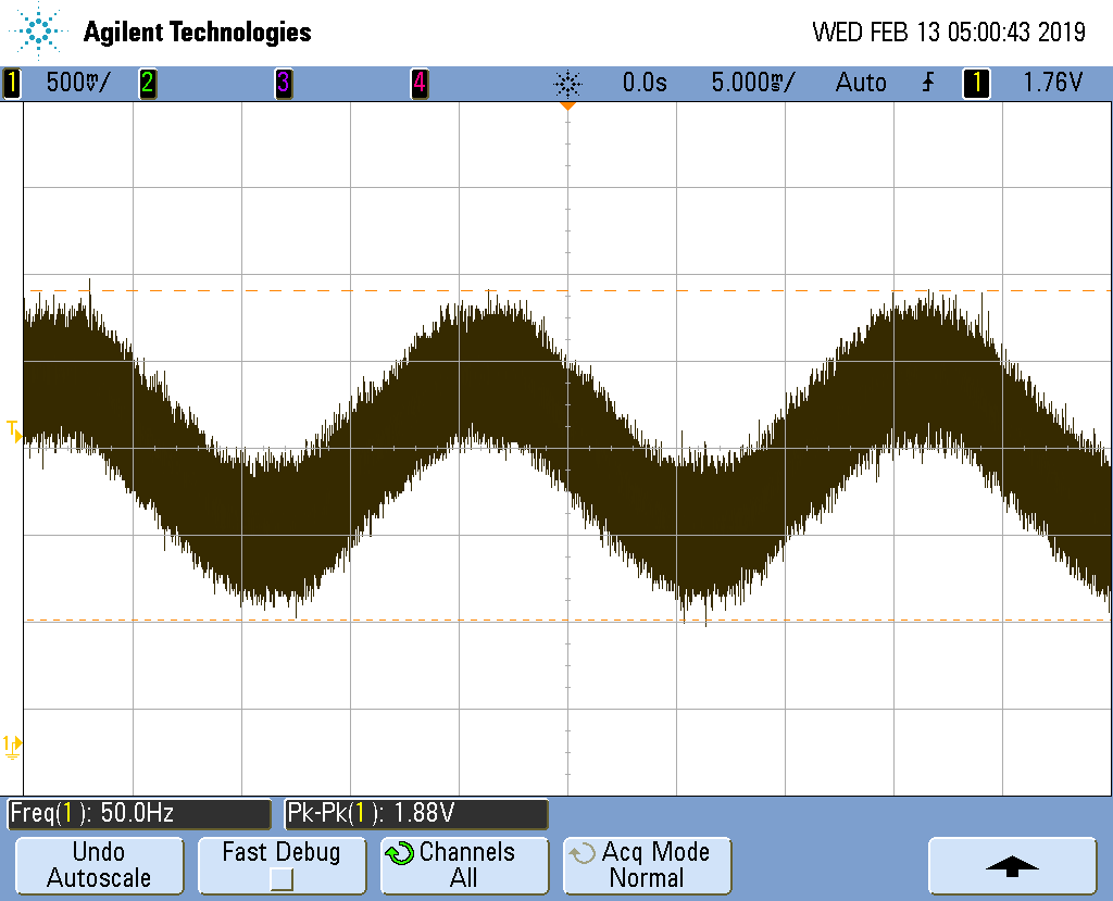
Hi Ian thanks for the reply. I’ve previously seen this reference and am prepared for the DAC to be poor but I’m measuring 3amps when no current is flowing. The trace on the oscilloscope is showing a few hundred millivolts so I’m not surprised at this - what I dont understand is why my trace is so noisey. One IO turn the heater on I get much better readings however the trace is still all over the place!
Here are 3 traces, one at 0amps input the other at 1/2 heat and full heat. The probe is on the io pin and the gnd is to the ESP32 gnd.
I had a pretty similar experience a few years back when I prototyped a PiHat and found an old thread that mentioned a cap on the op amp output, that seemed to fix it for me. IIRC Robins early designs had the cap on the op amp output too.
More recently, although I don’t recall when or where (stm32 thread?), I have a faint recollection that @Robert.Wall made a passing comment about a cap on the output with ref to a spec (operating freq maybe?) I’m sure he will be able to confirm if that might (or might not) be worth trying.
Errr! Now your asking! From memory!!! I think it was to gnd, but I think you should either hunt out those discussions on the old forum or wait for some wise words from someone like Robert that know for sure.
My point was, there is further info out there regards the use of a further cap to help you find a resolution, rather than specifically “fit a cap”.
Yes, it is to decouple the op.amp. output to ground. The value should only be as large as it needs to be (hardly a purchasing spec., I know!) so I’d start around 1 μF.
The problem is going to be that your op.amp. is too good - and you’re adding some feedback via stray capacitance or a shared conductor that’s turned it into an oscillator.
Thanks Robert and Paul - yes this worked a charm. I’ve put a 1uF SMD ceramic in and that has flattened the noisy trace. Another issue that was that the Agilent scope (borrowed) seems to have its own problems as I tested it on the square wave output and that was not clean either - I even tried different channels and different probes but it looks like it needs some repair. I had to dig out my hand assembled $20 jytech scope to get the results!
Separately I found this resource regarding the ESP32 ADC accuracy:
Further down this long page it gos into some detail on how to improve ADC accuracy by applying a 0.1uf cap across the input to GND. I also did this and this improved the situation to the point that the quiescent reading (0 amps flowing) to under 200mA which, given these readings is difficulty on an AC signal I’m happy to live with.
Also I note from the document that since some time in 2018, unique calibration values have been fused into each chip to improve the readings further. Currently the board I have seems to be have the ADC reference voltage loaded but not any slope correcting values.
Perhaps my ESP32, 12bit readings are as good as an Arduino 10 bit ADC?!
Looks great.
Here’s something I found while researching for the stm32 project here. It’s from an ADE series energy monitor IC datasheet.
The bottom half is different on ours, so only one burden and one cap are used. The cap to GND and the burden to bias as you have it.
That diagram is for a 7kHz cutout.
Yes, one of the nice things about those energy ICs is you can feed them the +ve and the -ve swing… no need for any mid-rails to be built. Obviously you don’t want to be doing that on a general purpose cpu though.
And one other tip is to put the same LPF on all your inputs (including V)… that way they all cop the same phase error together.
Ok I’ve revised the schematic to include low pass (ant-aliasing) filters on each input. I also added a DC input 2.5mm jack as an alternative to the usb on the ESP board.
Other changes
Added a 2nd row of holes for the dev board. Some are 0.9" and the official one is 1.0" Doh!
split the top flooded layer between 3,3v and 5v
Provided a vouple of hook up points for probes (TestAC and TestDC)
C5 and C6 might cause issues, but there’s no harm in leaving the pads in. That’s what we did for the stm, just left a pad for a cap if needed, it wasn’t in the end.
C6, the cap to ground was needed (and suggested by Robert above). My traces had lots of high frequency. noise on them. This cap quietened them down a lot. Not sure about C5 though, the diagram in the Learn section say’s this cap can be reduced to 100nf for high value voltage divider resistors but I’m using 12k so I assumed the 1uF was needed? Anyway, thank you very much for the feedback.


 , but a board revision number would be a good idea (couldn’t see one).