I’d like to replicate the voltage sampling block of EmonTX 3.4 for a small project. The simple schematic here is working fine, I’ve used it in the past. Now I have taken a look at the latest actual schematics, and I don’t really get how it works. I must be tired and miss something very basic.
First, how is the divided secunder voltage offset with the mid-3.3V value? There doesn’t seem to be a connection from the input to both ends of the divider net.
Second, shouldn’t C17 be an AC type cap? It doesn’t look there are guarantees of cutting reverse voltages to it…
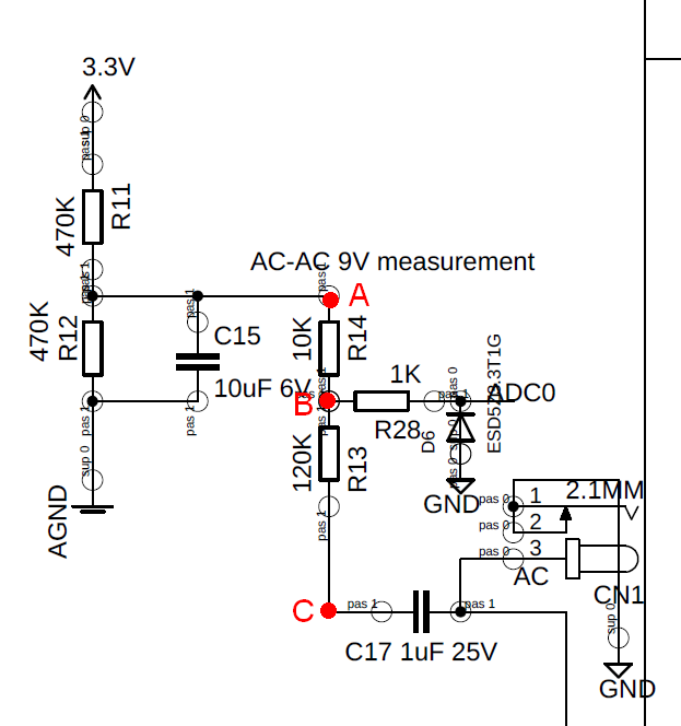
The first thing you must understand is the a.c. input to the emonTx V3.4 is also a power supply. That is not the case, and it never can be the case, with the “simple schematic” arrangement that was used before the emonTx V3 appeared.
The emonTx V3 arrangement is two very simple circuits that are superimposed on each other. If you ignore the measurement side, the power supply is a simple half-wave rectifier using D1 and C18 to provide a supply for the MCP1754 regulator. R29 is there to limit the current so as not to put too big a dent in the a.c. wave that you are trying to measure.
The measurement side is then exactly the same as any audio amplifier where the source signal is referenced to ground. The alternating voltage from the a.c. adapter is a.c. coupled via C17 and divided down by R13 & R14, with R11 & R12 with C15 providing the mid-rail bias voltage. R28 is there to limit the current in the protection diodes, and plays no part in normal operation.
There is not - at d.c., but of course there still is to a.c., via C15. Yes, really: C15 puts the ‘bottom’ end of the divider at an a.c. ground, the same as the sleeve of the a.c. input connector - and that’s an a.c. ground as well as a true ground.
If you carefully check the voltages, there is always a positive voltage applied to it, so there is no need. And of course, a 1 µF non-polarised capacitor would be huge, and would be expensive to fit, probably needing to be done manually.
Thanks for the (always) thorough explanation. Now… If I understand it well, then the AC voltage at ADC0 is inverted in phase (compared to the source AC), right? If not, then I’m still missing something very basic.
How can that be? There is nothing in there to invert the phase. The ADC input is in phase with the voltage at the centre pin of the input connector, to within something like 0.05°.
Even if there was a signal inversion, a simple multiply by -1 in the software would correct it.
OK… I’m simplifying the numbers a bit. Also, let’s ignore the power supply part now. Please also see the attached image.
A is fixed at 1.65V. C is the AC input (transformer secondary voltage), which when referenced to ground, is swinging between -13V and +13V. We essentially measure the voltage difference between A and C, divided down to suit the ADC.
B = (C - A) * (10 / 130). [simplification: 10 / 130 = 0.077] When input is at the minimum voltage, B = (-13 - 1.65) * 0.077 = -1.128V. When input is at the maximum voltage, B = (13 - 1.65) * 0.077 = 0,874. The full voltage swing appears to be around 2V at the input of the ADC. It’s also asymmetric (which should not be a problem with AC). Where is my mistake? It seems so basic EE stuff, yet I fail to grasp something very essential.
Thanks. That’s not twice, I just simplified the expression to a real number in a separate sentence. I’ll add some parentheses to ease the confusion. Anyway, C17 seems to be the key here.
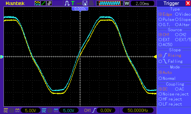
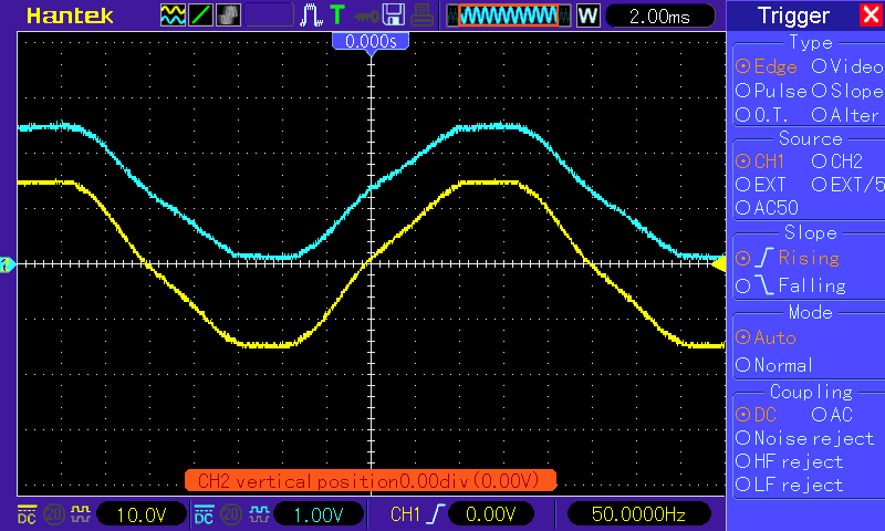
As promised. The yellow trace is the a.c. input, the blue trace is the other side of C17.
The first picture shows both at 5 V/div, for the second, the blue trace is at 1.0 V/div.
In the second picture, the 1.35 V d.c. shift is clearly seen.
You need to look at and analyse the a.c. conditions and the d.c. conditions separately.
Fundamental to that is the principle of superposition, which says that in a linear circuit (that’s important), you can analyse it for d.c. by taking the a.c. source away and replacing it by short circuit and replace each capacitor with an open circuit; then you put those back and instead analyse it for a.c: remove the d.c. source and replace that by a short circuit and each capacitor also by a short circuit. Then you add the two results together.
(That’s grossly oversimplified because I know the capacitance values are such that at the frequency we’re interested in, what I’ve written is a good enough approximation to understand what’s going on.)
If you want, you can download LTSpice, simulate the circuit, and explore its operation in detail.