Hello,
how does the function of the controller with this fake chip manifest itself?
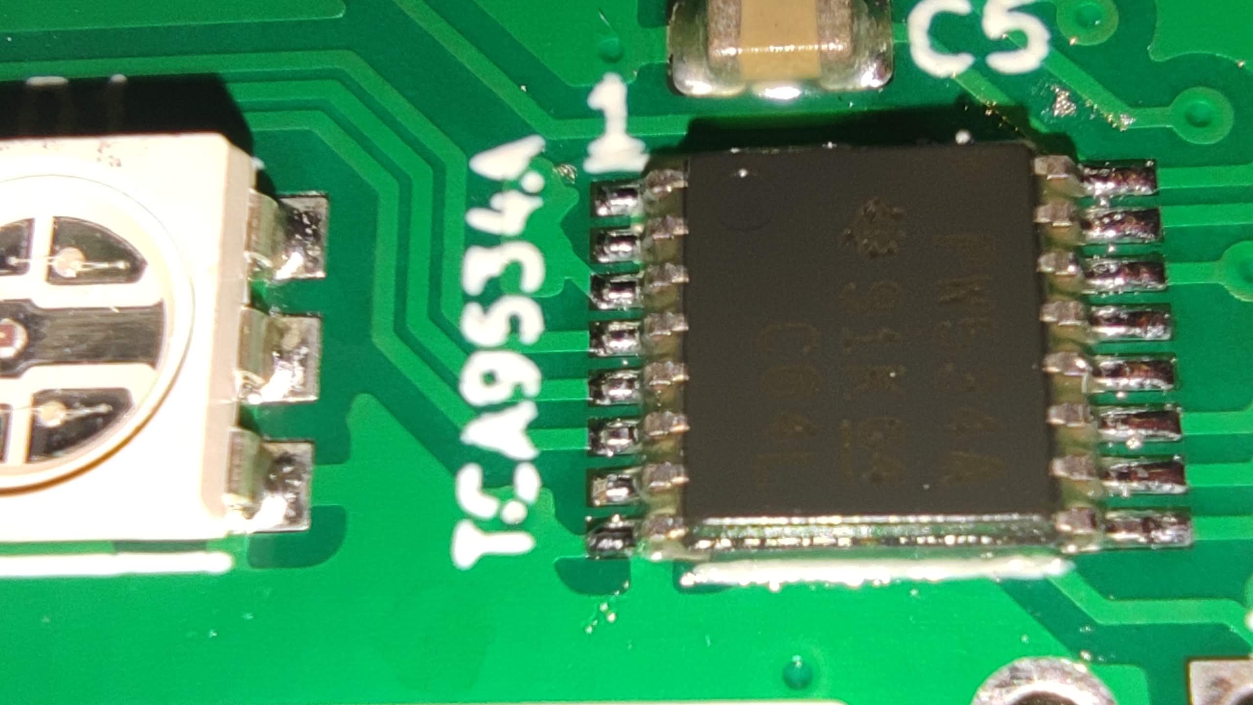
In my case, the TCA9534 chip somehow identifies itself.
[I] [HAL_ESP32.cpp: 232] ConfigureI2C (): Configure I2C
[I] [HAL_ESP32.cpp: 291] ConfigureI2C (): Found TCA9534A
[I] [HAL_ESP32.cpp: 321] ConfigureI2C (): Found TCA6408
But the LED (D1) does not light up in any way, even though everything else seems to be working.
Do not think that problem is in TCA9534A.
Check D1 LED orientation. Check solder joints of D1 and resistors near to it.
Take a picture with D1 LED, resistors, and TCA9534A clearly visible.
studying this part of the code now.
doesn’t look like there is any real imbalance check in there. Why do you think there is a 10mV limit???
what the code currently does, is report this “imbalance cells” warning when at least one cell starts balancing which is not particularly helpful.
For example my test bank is charging, range is 125mV, nothing reported on Victron. Once cells start balancing I get this warning. Same with discharging, you may end up with 200+mV difference, no warnings issued in Victron -check it out.
I’m trying to add the Range (as shown on top of the webserver screen) in the influxdb and then canbus code so I can monitor that and then change the warning/error codes for more detailed conditions.
Another example is that if you have a Cell under voltage rule set in your Rules, this is not issuing a warning or an error in canbus.
ATM it seems that in canbus we get a warning for balancing cells, and an error for Charge Voltage Limit as set in the Victron CANBUS integration section. We’ll have to add more to that for sure and I’m trying to work on this.
Eventually we’ll have to create either a replication of Rules for Victron, or select which of the diyBMS rules will be “exported” as warnings and which as errors in Victron.
Thanks for your answer, it makes sense, the 10mV thing did not get it from anywhere, I just thought it could be. I see that the code is clear and generates the warnings, as you say when it starts to download a cell.
If I agree with you, that this alert does not make sense, especially if it affects Victron to reduce the charge level, or at least not in the way it does. It is true that in this way it gives the system time to balance, but it generates unnecessary load reductions, since the unbalance range is too small to stop the load. On the other hand, I have observed that the cell that is the first of the 32 cells is punctually affected by an increase in voltage that is then adjusted (it receives the bulk of the load that is then transferred to the rest of the cells)
Hi Stuart, I’ve got a couple of questions about the v4.4 design. If these are answered earlier in this topic, I apologize in advance. I’m still working my way through. Anyway, here goes:
It appears the voltage measurement is being made at pin PA3, using a voltage divider to get into the range of the ADC set by the external reference. But the voltage divider (R3/R4) is dividing the ENABLE output of PA7, not the battery voltage or Vcc. Am I understanding the design correctly? And if so, what was your reason for using a microcontroller output pin rather than the power supplied to the board?
How did you decide on the balance current of 1+ amp? I assume I could reduce that current by choosing a different value for that array of 9 resistors, but what should I consider based on my application?
Reply for
1: Designed for lowest curent consumption - voltage on divider is only if is voltage on pin PA7. Measurement acurracy is litle low…
2: I used ceramic resistor for balancing current about 2A - minimum for my old battery pack. If you use resistrors for lowest ballance current, is only you way… Balancing current is temperature limited, in owerheat is downed from PWM.
P.S: mi little hardware upgrade: 10n ceramic smd capacitors placed directly to R4 and AZ432 - Its filtered HF interference, voltage measurement curve sended on MQTT is smoothing.
Thanks, @kodl1 . I’ve got a set of boards on order from JLCPCB, and I’ll see what the voltage from the I/O pin looks like on them all. Looking at the datasheet, if the “Hi” voltage is as low as the guaranteed value, it could be a major error source.
I’ve got a spreadsheet looking at how the various error sources could potentially add up - I’ll post it up here in a few days.
Did you get a resolution to this wifi problem? I’ve had very unreliable wifi connections from the controller to routers and access points. I can’t seem to get the web server in the mini d1 to be reliable and keep a connection - I’ve tried lots of different d1’s and routers, can’t seem to find an answer to it. Any advice?
There is a D1 with an external aerial - perhaps that will help you? If you have the TFT screen installed, it also provides the wifi signal strength in the bottom right corner.
Thanks everyone involved in the project, especially Stuart. Btw i wonder if the module could turn into bus bar between 2 lifepo4 battery? If so i would love to make 1, thanks
I don’t think I have signal strength issue as Mini D1 is about 5 meters away from Raspberry AP.
Though I did notice once again when AP was down for some wifi issues (more than 20 minutes) I needed to fix, Mini D1 was not able to connect back to it (no web interface nor sending data outside)
Also from time to time web interface struggles to load though it is still sending data to influxDB. After a minute or sometimes more it eventually does load up, but don’t think it is a wifi issue.
Though if you are using Raspberry Pi, there might be another issue related with number of wireless clients in AP mode Number of wireless clients in AP mode is very limited · Issue #3010 · raspberrypi/linux · GitHub
I was ordering 4.4 version modules and just got an email from JLCPCB that there is no 1.152mm SMT tooling holes on board. I have uploaded gerber file from there


