DIN Rail Meter development

Hello,

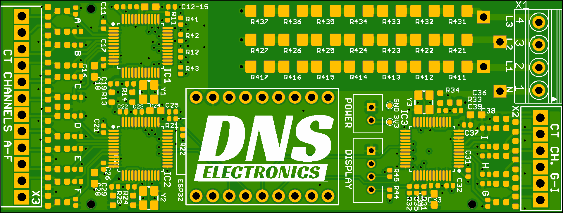
I’m currently developing my own DIN Rail Meter based on the Atmel ATM90E32 IC.
It should be 2 modules wide with 3 voltage and 9 current channels.

This is where I got my idea: GitHub - CircuitSetup/Expandable-6-Channel-ESP32-Energy-Meter: Hardware & Software documentation for the CircuitSetup Expandable 6 Channel ESP32 Energy Meter. Works with ESPHome and Home Assistant.
And this is my project: GitHub - denes44/DIN-Rail-Power-Meter

I would love to have a couple questions about the application of this IC if you can help me.
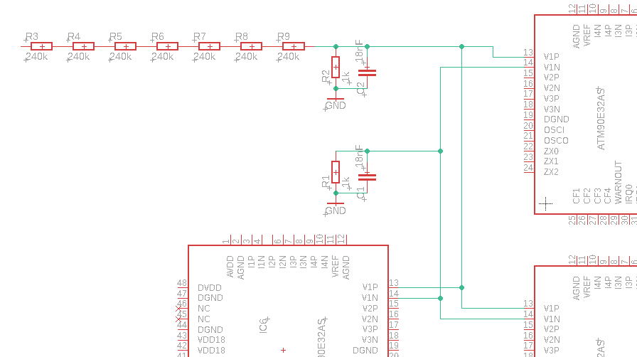
Voltage monitoring
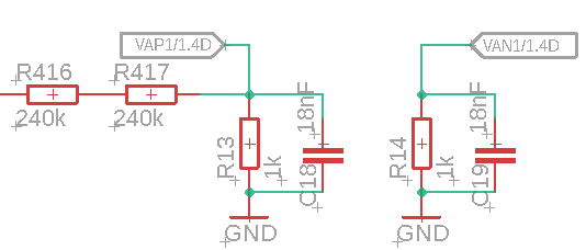
I decided to go with the resistor network from the application note to measure the voltage.
Mostly because of the size. And since the final device is meant to be installed inside the electrical cabinet and doesn’t have any outside interfaces, just the Wi-Fi I don’t think the lack of isolation will be a problem.

This is the voltage measuring circuit from the application note:


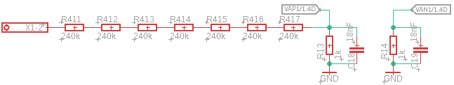
As far as I understand, this is “just” a voltage divider with a 1680k : 1k ratio.
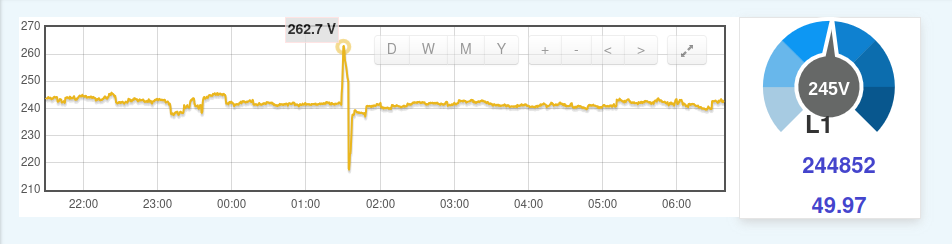
Wouldn’t the resulting voltage be too small? The maximum the IC can take is 720 mVrms.

The second question is that the resistor size (1206) is because of the voltage rating, not because the power rating, right? I assume I’ll need some good resistors here with a high power rating like the HV06W series from Uni-royal, 500V max. working voltage, 1/4W power rating.

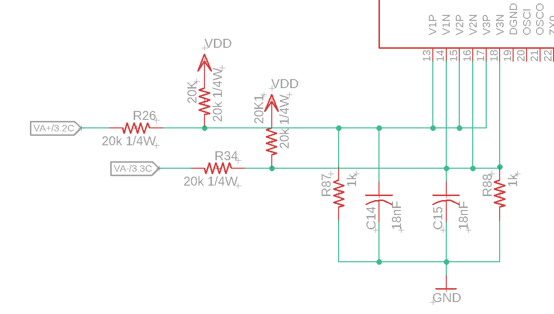
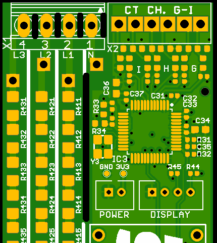
Multiple voltage monitoring for every IC
Right now the circuit is set up, that I have 3 ICs on the PCB, and each IC monitors the voltage of one phase.
So I have the output of the voltage divider connected to all three inputs of the IC:


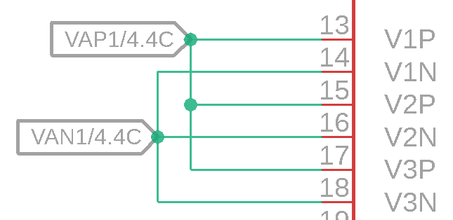
Technically it isn’t necessary, because I can configure it by software use the V1 input for for all 3 current inputs, but it doesn’t hurt, and the original project does it this way too.

The problem with this if somebody only wants to measure the total current of each phase, still all 3 ICs are needed on the PCB, it’s not possible to use a version where there is only one IC is needed (thus cheaper).
The other disadvantage could be in a 3 phase environment is that each IC can measure currents on one specific phase, so it’s 3 current channels per phase, I cannot do for example 8-1-1.

To overcome this, I plan to connect the 3 phases to every IC, so the L1 would be V1 on IC1,2,3; L2 would be V2 on IC1,2,3 and L3 would be V3 on IC1,2,3.

The question is do I need to duplicate any component to do this? Like a separate capacitor for every IC, or anything like this.
Or I can just connect the “output” of the voltage divider, VAP1, to the V1P input of all ICs parallel, like I do now with the V1-2-3 input on the same IC?
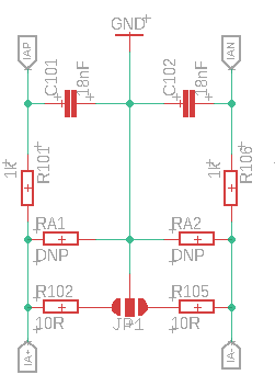
Circuit monitoring
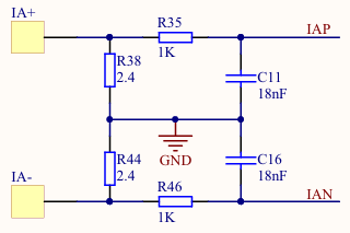
This is the current measuring circuit from the application note:


And this is from the github project:

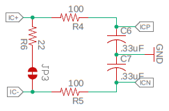
There are two key differences, one is the value of the R4/5-R35/R46 and the C6/7-C11/16.
I assume these are just an RC low-pass filters, and doesn’t really modify the measurement value, right?
I tend to go with the values from the application note, but JLCPCB doesn’t have a 18nF capacitor as a basic part, so I’m planning to change it to 22nF. That shouldn’t make too much of a difference, right?

The other thing is the burden resistor. On the second circuit it’s clear that it’s R6.
On the first one I assume the R38 and R44 resistors are the burden resistors, but why they are connected this way, so the middle point is connected to GND?

I’d agree. But clearly, this won’t apply while you’re working on it during design and testing.

If you are publishing the design (as the writer of the App Note), then you probably need to make it workable for the great majority of electricity supply systems. For example, ours in the UK has a maximum legal limit of 254 V rms, but it is known to go higher sometimes in some areas, and on top of that you can have spikes from switching. At 254 V in, you’d expect about 150 mV rms at the ADC input - but it will only drop to about 80% of this in normal use, unlike the current inputs where the minimum you might want to measure could be 5% or even less of the maximum. I would follow the data sheet / app. note.

Almost certainly yes, because if a resistor goes open-circuit, the peak supply voltage appears across the two ends. And this applies to your p.c.b tracks too, so they must be spaced correctly.

I’m not quite sure what your objective is here. If you have 3 × Atmel ATM90E32, and you connect each line voltage to all three i.c’s, you’ll have the 3 voltage and 9 current channels you ask for. Clearly, the i.c. is designed as a 3-phase device, to measure a single 3-phase supply, so why not use it like that? If you can pair any current channel to any voltage channel in software (like we can with emonLibDB), then you can do that across all 3 i.c’s, and have 3 - 3 - 3, or 9 - 0 - 0, or anything in between.

This is exactly what I think the designer would have expected. (If it makes the p.c.b. layout easier, it doesn’t have to be exactly like that, it could be 1-2-3 on i.c’s 1 & 3 but 3-1-2 on i.c 2, but it will make the software more ‘obvious’ if you do.)

I’d need to study the data sheet for a long time to find if there is a reason not to do as you suggest, but it does feel wrong to me. For the cost, I’d have 9 voltage divider chains. If nothing else, a fault in one won’t affect the other 2 on that phase.

They are a bit more than this, they are also anti-alias, and ideally voltage and current channels should be matched - as they are in the app. note. You’ll lose some of the higher harmonics if you change the 18 nF to 22 nF, it might not worry you - it’s your choice (but I think the filter is outside the normal range of frequencies you’d be interested in anyway).

Correct, they are the burden, and it is to ground the c.t, - most likely for both safety and interference suppression reasons, so any interference sees a balanced impedance to ground and is therefore rejected by the differential input of the i.c. (yes, it’s not widely understood that a balanced input means balanced impedances, not necessarily balanced signal voltages; so it’s the interfering voltages on the two legs that are equal, to correctly suppress interference).

Thank you for your very detailed reply!

I think I will use the values from the application note, because I’m not considering myself to know better. :slight_smile:
I was just curious why did they chose this value, because it produces so low voltage (even when a line to line measurement happens because of mis-wiring) compared to what the IC can do.
But it’s probably because the accuracy is still enough for the voltage measurement, and this way they have a good amount of reserve volt over-voltage situation.

Well, what the original CircuitSetup’s github project is that the same voltage was connected to all three voltage channels, so you did not had to do any software configuration in a 1-phase system.
The board is modular, and if you wanted to do 2-phase or 3-phase, you used more boards.
But then it can only could do a 3-3-3 distribution of the current channels, because every IC could only monitor one voltage.

Right now I do the same, except my board is not modular, I have 3 ICs and 3 voltage input, but every voltage input is dedicated to one IC.

I’m thinking about a design where every IC gets all 3 voltage inputs, so somebody can use a circuit by only soldering one IC if they only need 3 current channels.
This might make the software complicated, I’m not sure I can will be able to do this by esphome in a way that I won’t need separate firmware files, but that’s another problem.

That would be very difficult to fit into the 2 module DIN enclosure, the PCB is very full as it is already.

This is how the other project did it (it uses the output of the transformer, rather than voltage divider):


Here the voltage is connected to all 3 inputs, with only one anti-aliasing circuit, and it seems to be working fine for them.

I think it doesn’t matter if I connect the same voltage circuits to 3 inputs on one IC, or to one input on every IC, right?

So like this:

I can only refer to CircuitSetup’s design, where the RC filter was purposefully lowered to 100 Ohm and 330 nF, making the cutoff frequency from 8.8 kHz to 4.8 kHz.

I’m afraid to be so drastic here, but I think according to this, the 22 nF instead of the 18 nF should be fine.
The ATM90E26, the 1 phase version of the IC uses 1 kOhm and 33 nF in the application note.

Ah, okay, so it seems like the better way to do it.

But this can only be done with CTs that doesn’t have a burden resistor, the ones that have one built in (assume I don’t have burdens on my PCB) will work, but with a slightly less toleration for interference, right?

I’m wondering how much of a difference does it make, because it would be easier to design the PCB with only one burden resistor.

To answer that question fully, you would need to know the exact circuit arrangement of the input amplifier in the i.c. If it is satisfactory for the three inputs of one i.c, it does not mean it will be same for the amplifiers in 3 different i.c’s. I think the only way you will find out if there is a problem will be to build and test it.

The data sheet says “The M90E32AS incorporates 6 independent 2nd order sigma-delta ADCs, which could be employed in three voltage channels (phase A, B and C) and three current channels (phase A, B, C) in a typical three-phase four-wire system.” Two important words here are “independent” and “could”. It’s detailed in section 3.4 ANALOG/DIGITAL CHANNEL MAPPING, so by putting the correct values into the voltage and current mapping registers, you can link the voltages and currents to the power calculation in any way you want.

No, you can do it with a c.t. with a built-in burden. You can either use the circuit for a Rogowsky Coil (which in effect ties it to ground at a.c. but not d.c.), or you will need to guess the value of the burden resistor (or ask the manufacturer) and then you can use two resistors whose values are much greater than this. You will slightly reduce the output (i.e. change the calibration) of the c.t, which you can correct in the software. My guess is the burden will be in the range 50 - 500 Ω, so if your “R38” & “R44” are each 50 kQ, you will inject only a 0.05% to 0.5% error, and your c.t. will be tied to ground.

Agreed, but you will only know when you have the problem. :anguished: Again, I think you can believe that the people who wrote the data sheet and application note have tested both, and know which is best.