Calibrate phase with samples shift

Greetings,

I have successfully installed 1 EmonTx on my house , all is neat & clean. Now , inspired in learning the underground logic behind OEM system , i want to make a custom device based on a STM32F103C8Tx MCU (BluePill board) , i’m using the CT circuit adapted to 3V3 levels and I have accidentally ordered a big banch of ZMPT board, “the rubbish module” as stated by Robert in a comment ^^ , so as i understood from previous topics , the big problem of ZMPT module is the huge phase shift introduced with the electronics around the ZMPT CT. Which makes the phase calibration process tedious.
I did an order to bring some high voltage resistors to build the simple voltage sensing as explained by Robert in a comment.
Now , waiting the items to be received , i tried to bring it in phase with the method i will describe below.
First the hole system configuration of my setup is the following :
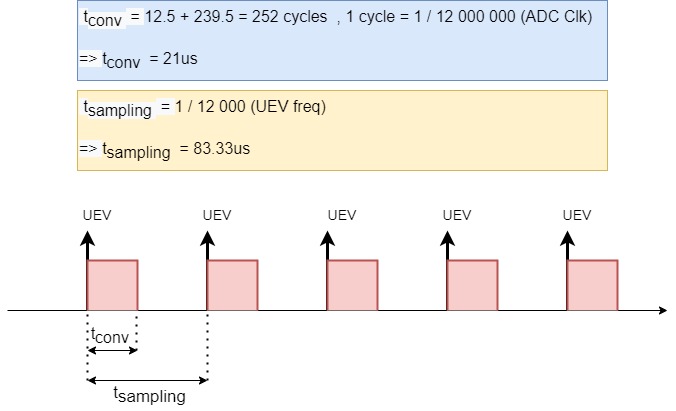
1- The timer clocks the ADCs at 12Khz , the ADCs are in dual mode , they start the sampling at the same time, then data is sent in a 32-bit word to a buffer , containing both raw values for current & voltage

2- As you can see the continuous mode is disabled so that only the timer can trigger the conversions , 12 khz is suited as it gives the ADC enough time to finish the conversion :slight_smile:
stlm32_zmpt_ct-sampling_timing

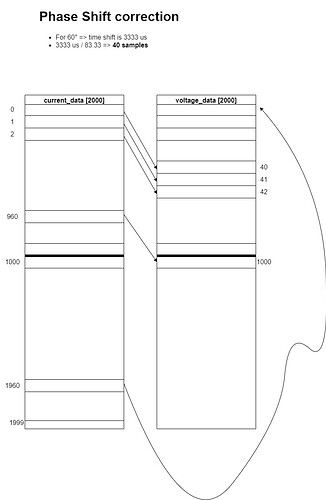
3- To simulate phase shift correction , I’m using resistor load to play with the phase.To do the correction , I’m only introducing a specific order for power calculation , I shift the samples by a specific offset based on the phase error . Here is an example for 60° error :

4- My code is mainly based on the code in Emon3CT_CB_v2 , the main change is the offset in the voltage sample => (offset + i + 40)%2000 .

Now I’m not sure if the above is an accurate method , I will be helpful for any remark that i may have missed. Could I use this to stay with the ZMPT board and still have consistent values ?

#define VDD_APPLI                      ((uint32_t) 3300)    /* Value of analog voltage supply Vdda (unit: mV) */
#define RANGE_12BITS                   ((uint32_t) 4095)    /* Max digital value for a full range of 12 bits */
#define ADCCONVERTEDVALUES_BUFFER_SIZE ((uint32_t) 2000)    /* Size of array containing ADC converted values */
#define true 1
#define false 0
#define MID_ADC_READING 2048

/* USER CODE END PD */

/* Private macro -------------------------------------------------------------*/
/* USER CODE BEGIN PM */
#define COMPUTATION_DUALMODE_ADCMASTER_RESULT(DATA)                 \
  ((DATA) & 0x0000FFFF)
#define COMPUTATION_DUALMODE_ADCSLAVE_RESULT(DATA)                  \
  ((DATA) >> 16)
uint32_t time2;
uint32_t time1;
uint32_t time_diff;

// Serial output buffer
char log_buffer[250];

// Flag
bool readings_ready = false;

// Calibration
float VCAL = 808.02;
float ICAL = 88.49;


// Number of waveforms to count
uint8_t waveforms = 250;

// accumulators
typedef struct dataMeter_
{
  int64_t  sum_P;
  uint64_t sum_V_sq;
  uint64_t sum_I_sq;
  int32_t  sum_V;
  int32_t  sum_I;
  uint32_t count;

  uint32_t positive_V;
  uint32_t last_positive_V;
  uint32_t cycles;
} dataMeter_t;

double Ws_acc = 0 ; // Watt second accumulator
static dataMeter_t dataMeter;
static dataMeter_t dataMeter_copy;
__IO uint32_t   aADCDualConvertedValues[ADCCONVERTEDVALUES_BUFFER_SIZE];

void HAL_ADC_ConvHalfCpltCallback(ADC_HandleTypeDef* hadc)
{
  process_frame(0);
}

void HAL_ADC_ConvCpltCallback(ADC_HandleTypeDef* hadc)
{
 process_frame(1000);
}

void process_frame(uint16_t offset)
{
  int32_t sample_V, sample_I, signed_V, signed_I;
  for (int i = 0; i < 1000; i++)
  {
      dataMeter_t *data = &dataMeter;

      // ----------------------------------------
      // Voltage
      sample_V = COMPUTATION_DUALMODE_ADCMASTER_RESULT(aADCDualConvertedValues[offset + i ]);
      //voltageValues[offset + i] = sample_V;
      signed_V = sample_V - 1064;
      data->sum_V += signed_V;
      data->sum_V_sq += signed_V * signed_V;
      // ----------------------------------------
      // Current
      sample_I = COMPUTATION_DUALMODE_ADCSLAVE_RESULT(aADCDualConvertedValues[(offset + i + 40)%2000]);
      //currentValues[offset + i] = sample_I;
      signed_I = sample_I - MID_ADC_READING;
      data->sum_I += signed_I;
      data->sum_I_sq += signed_I * signed_I;
      // ----------------------------------------
      // Power
      data->sum_P += signed_V * signed_I;
      // ----------------------------------------
      // Sample Count
      data->count++;
      // ----------------------------------------
      // Zero crossing detection
      data->last_positive_V = data->positive_V;
      if (signed_V > 5)
      {
        data->positive_V = true;
      }
      else if (signed_V < -5)
      {
        data->positive_V = false;
      }

      if (!data->last_positive_V && data->positive_V)
      {
        data->cycles++;
      }
      // ----------------------------------------
      // Complete Waveform Cycles to count
      if (data->cycles == waveforms)
      {
        data->cycles = 0;

        dataMeter_t *data_copy = &dataMeter_copy;
        // Copy accumulators for use in main loop
        memcpy((void *)data_copy, (void *)data, sizeof(dataMeter_t));
        // Reset accumulators to zero ready for next set of measurements
        memset((void *)data, 0, sizeof(dataMeter_t));

        readings_ready = true;
      }
	  //float Vmeantemp = data->sum_V / (float)data->count;
      //printf("mean V %f \r\n",Vmeantemp);
  }
  }


void TurnOnBuiltInLED(void) {
	  HAL_GPIO_WritePin(LED_GPIO_Port, LED_Pin, GPIO_PIN_RESET); // On LED
}
void TurnOffBuiltInLED(void) {
	  HAL_GPIO_WritePin(LED_GPIO_Port, LED_Pin, GPIO_PIN_SET); // On LED
}
/* USER CODE END 0 */

/**
  * @brief  The application entry point.
  * @retval int
  */
int main(void)
{
  /* USER CODE BEGIN 1 */

  /* USER CODE END 1 */

  /* MCU Configuration--------------------------------------------------------*/

  /* Reset of all peripherals, Initializes the Flash interface and the Systick. */
  HAL_Init();

  /* USER CODE BEGIN Init */
  float V_RATIO = VCAL * (3.3 / 4096.0);
  float I_RATIO = ICAL * (3.3 / 4096.0);
  /* USER CODE END Init */

  /* Configure the system clock */
  SystemClock_Config();

  /* USER CODE BEGIN SysInit */

  /* USER CODE END SysInit */

  /* Initialize all configured peripherals */
  MX_GPIO_Init();
  MX_DMA_Init();
  MX_ADC1_Init();
  MX_ADC2_Init();
  MX_I2C1_Init();
  MX_TIM3_Init();
  MX_USART1_UART_Init();
  /* USER CODE BEGIN 2 */
  HAL_ADCEx_Calibration_Start(&hadc1);
  HAL_ADCEx_Calibration_Start(&hadc2);

  HAL_TIM_Base_Start(&htim3);

  HAL_ADC_Start(&hadc2);
  HAL_ADCEx_MultiModeStart_DMA(&hadc1, aADCDualConvertedValues, ADCCONVERTEDVALUES_BUFFER_SIZE);
  //to fix first time loop issue
  time1 = HAL_GetTick();
  /* USER CODE END 2 */

  /* Infinite loop */
  /* USER CODE BEGIN WHILE */
  while (1)
  {
	  if (readings_ready)
	  {
		readings_ready = false;
		time2 = time1;
		time1 = HAL_GetTick();
		time_diff = time1 - time2;

		dataMeter_t *dt = &dataMeter_copy;

		  float Vmean = dt->sum_V / (float)dt->count;
		  float Imean = dt->sum_I / (float)dt->count;

		  dt->sum_V_sq /= (float)dt->count;
		  dt->sum_V_sq -= (Vmean * Vmean); // offset subtraction

		  if (dt->sum_V_sq < 0) // if offset removal cause a negative number,
			dt->sum_V_sq = 0;   // make it 0 to avoid a nan at sqrt.

		  float Vrms = V_RATIO * sqrtf((float)dt->sum_V_sq);

		  dt->sum_I_sq /= (float)dt->count;
		  dt->sum_I_sq -= (Imean * Imean);

		  if (dt->sum_I_sq < 0)
			dt->sum_I_sq = 0;

		  float Irms = I_RATIO * sqrtf((float)dt->sum_I_sq);

		  float mean_P = (dt->sum_P / (float)dt->count) - (Vmean * Imean);
		  float realPower = V_RATIO * I_RATIO * mean_P;

		  float apparentPower = Vrms * Irms;

		  float powerFactor;
		  if (apparentPower != 0) // prevents 'inf' at division
		  {
			powerFactor = realPower / apparentPower;
		  }
		  else
			powerFactor = 0;

		  Ws_acc += ((float)(time_diff / 1000.0)) * realPower; // Watt second accumulator.
		  float Wh_acc = Ws_acc / 3600.0;                      // Wh_acc
		  float frequency = 250.0 / (float)(time_diff / 1000.0);    // Hz
          int _n = 1;
		  sprintf(log_buffer, "V%d:%.2f,I%d:%.3f,RP%d:%.1f,AP%d:%.1f,PF%d:%.3f,Wh%d:%.3f,Hz%d:%.2f,C%d:%ld", _n, Vrms, _n, Irms, _n, realPower, _n, apparentPower, _n, powerFactor, _n, Wh_acc, _n, frequency, _n, dt->count);
		  printf(log_buffer);
		  printf("\r\n");
	  }
    /* USER CODE END WHILE */

    /* USER CODE BEGIN 3 */
  }
  /* USER CODE END 3 */
}

There are two points there. First, if you make a direct galvanic connection to the electricity supply, the entire project including any connected computer (say for programming or calibration) must be treated as LIVE and you must take the appropriate safety precautions. Secondly, the phase error introduced by the, probably unnecessary, filters is huge. It seems rather pointless to introduce complexity into the software when you could remove the filters and use the transformer on its own, with very little phase error. Having said that, the principle of having two arrays with a time delay between them is sound, but you must bear in mind that phase and time are not quite the same thing, and you might need to adjust the delay if your line frequency is not closely regulated - simply because the delay is a significant portion of a complete cycle.

Is there any alternative to a direct galvanic connection ?

Yes, three choices immediately spring to mind.

1. What you have in the ZMPT101.

This is a current transformer with two windings. By using a multiplying resistor in series with the primary winding, the primary current can be made proportional to the voltage across both, then you use the burden in the normal way to convert the secondary current into a voltage to go straight into your ADC. The data sheet claims 0.2% linearity and a phase error of less than 20 minutes of arc.

  1. A purpose-made voltage transformer, e.g. SPT-0375 Potential Transformer Output Proportional Input Magnelab

  2. A capacitive “voltage transformer” which I proposed many years ago for a special case - search the archived forum for that. It comprises a low value capacitor created by wrapping foil around the line conductor, in series with a higher value capacitor giving a capacitive potential divider, then a very high input impedance amplifier to avoid making a R-C filter giving a phase shift.
    (“Capacitive” v.t’s are widely used on high voltage transmission lines.)

Thank you Robert for the detailed answer , you are the best

@Robert.Wall : I decided to go ahead with the first option it seems promising.
Using 2* 65Kohm as limiting current in series and 1* sampling resistor of 525Ohm will give 90% of a 3V3 ADC.
Now i’m curious about the type of that resistor , a 1% 1/2W Metal Film resistor is suited for such voltage in the high voltage end ?
A fast calculation gives around P = 260v^2 / 65k = 1.04 W , am i doing the math right ?
Also ,as we are in the 260V rating , how to choose the right resistor that can handle such voltage ? or it’s all about the power only ?

You should not be looking at A resistor, but several in series. It is easier to get a lower rated voltage resistors, and it one goes short-circuit (however unlikely that might be) you still have others in series to limit the current.

Where does your value of 65 kΩ come from? According to my sources, your mains voltage is 220 V, 50 Hz. The rated current of the c.t. is 2 mA, so at 220 V + 10%, the series resistance would be 121 kῺ. I would use 4 × 33 kΩ in series. At your nominal voltage + 10%, each would have approximately 60 V across it, the power in each would be about 0.11 W. For safety and long life, I would use 0.5 W resistors.

Again at nominal voltage+10%, the current is 1.833 mA, which is also the secondary current. therefore your burden will be (using my magic number 1.1 V for the rms voltage taking component tolerances into account) exactly 600 Ω. Even using a 560 Ω resistor (giving you 2.9 V peak-peak), will not degrade the performance of the voltage input, because unlike current, the range over which the (rms) voltage changes is minuscule when compared to the current.

You must still remember that the 4 resistors, their interconnections and the primary winding of the c.t. and its connections are all LIVE to mains voltage, and must be shrouded to prevent contact.

the primary winding logic make total sense to me.
For the secondary winding , i see that 560 Ohm sampling resistor will give a 1.02V rms voltage to the ADC (taking into account the current to be 1.833 mA). It seems to me like I’m not tacking advantage of the 3V3 - 10% of the ADC interval. From another perspective, the full range of ADC to be used is 90% of 3V3 , around 2.97V , which gives 1620 Ohm with 1.83mA. What I’m missing over here ?
EDIT : i’m missing the full swing of the signal apparently , as the U * 2 * sqrt(2) = 2.97 , since it’s a sine.

Indeed - for a 3.3 V ADC input range, the maximum rms voltage is a little over 1.1 V - subtract from the nominal 3.3 V range percentages for the accuracy of the ADC reference/supply (may be low), error in the burden (may be high), the centre bias voltage might be offset a little from the true centre, and you end up with about 1.1 V rms, my “magic” number.

For a voltage, calling it a sine wave is a reasonable approximation. For a current, that is not something that you should assume until you know the nature of the load.

1 Like

Many thanks for all the clarifications.

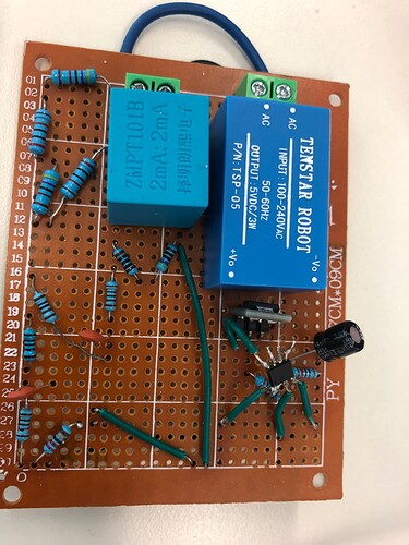
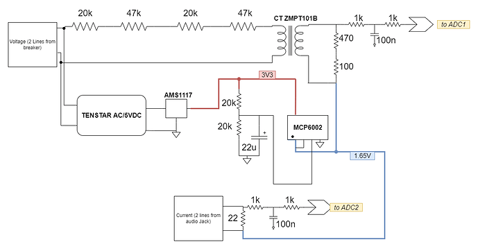
Hello @Robert.Wall , i’ve just finished the volage sensing circuit with ZMPT101B CT you described here
Could you please have a look to the final schematic for any remark or recommandation :
-I have used the bias buffering recommanded on the learn section (with MCP6002).
-I have added a 1k resistor as i’ve seen it in the emontx3 hardware files (to limit current ?)
-I have also added an RC filter so the Shannon will stay happy (anti aliasing as stated in the learn section too).

  • AMS1117 is used to give the 3V3, TENSTAR module to give 5V out of the AC.
    -AC line is mapped to TENSTAR to give energy to the whole board (is’t okey to do so ? i mean on the accuracy of measurements ).


There’s nothing that immediately stands out as being wrong, but what I would do (maybe I’m being over-cautious) is clean away all the copper pads between the high voltage side and the low voltage side, i.e. around the multiplier resistors, the mains connections to the power supply and underneath the ZPMT101B in particular, so that you have clear area of board (ideally at least 8 mm wide) separating the high voltage side from the low voltage side.

The impedance of your supply should be low enough for that not to matter. If it isn’t, this is the least of your problems. :open_mouth:

You will still need to nullify the effect of the phase error of the c.t, you can either delay using the readings after you’ve grabbed them, or you can delay triggering the ADC to take the reading. Which way you do it, or which is the better (or even possible) depends on a number of factors - how much memory and processing power you have, clock and sample rates, etc.

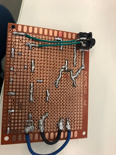
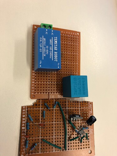
I don’t think Robert is being over-cautious at all. I think it’s actually quite dangerous as it stands. Those transformer and PSU designers will have (hopefully) gone to some length to ensure reinforced isolation between the primary and secondary sides. The layout as it stands undoes their hard work. All those copper pads on the underside are very close together. From a safety point of view, your total gap will be the sum off all the tiny gaps between them.

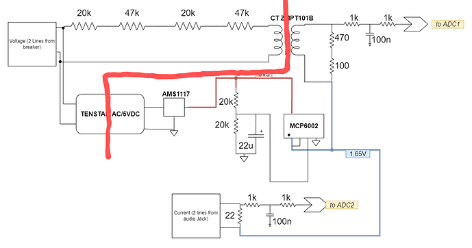
It helps to show the isolation barrier on the schematic as a constant reminder of what’s on the scarey side and what’s on the safe side. So yours would look like:

There should be no copper under the red line, and only those two components should traverse it. It should be 6.4mm to 8mm wide, depending on where on the grid you plan installing it. You could also consider cutting a slot out of the board.

Also, you need 3mm between your L and N terminals, they look way too close and are effectively even closer when you see the copper pattern underneath them. How big is the gap between the copper pads… 0.5mm? Looks like there are two gaps between L and N, so effectively they’re only 1mm apart?

Thanks for you both , i didn’t pay attention to those safety rules regarding AC.
@dBC your are right about the L & N distance, it’s only 1mm. I should redo all the high voltage work on a separated board without copper under.
Even the glue gun won’t help is this case ? (I mean for the part of removing the copper )

I use a 3mm wood chisel, held very nearly flat, and pare the copper away a narrow slice at a time. You could try a hot soldering iron to melt the glue first, but a sharp chisel is fairly quick and clean, and doesn’t risk leaving traces of carbon, which you might get with too much heat. And traces of carbon will be as bad or worse than the copper.

Got it, I’ll post my progress for instance.
Thanks for the warnings.

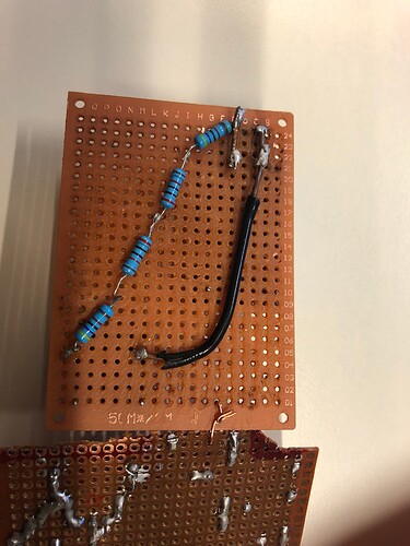
Using a wood chisel as suggested to remove copper underneath PSU and CT.
Now 4mm between L & N.


That’s still not very much. 4 mm of air is good, but 4 mm of paxolin that might be damp or dirty and provides a surface to the current to track across is not enough.