I’m in the process of building this. I just wanted to share this idea, and get some feedback. There are lots of reasons to use a nano and to include the esp8266. You can run a nice colour display, you can use the wifi to log data. You can also use the esp8266 to connect to weather underground and make decisions about whether to draw grid power after some cloudy days. The Nano is also pretty cheap on e-bay removes the need to buy crystals etc.
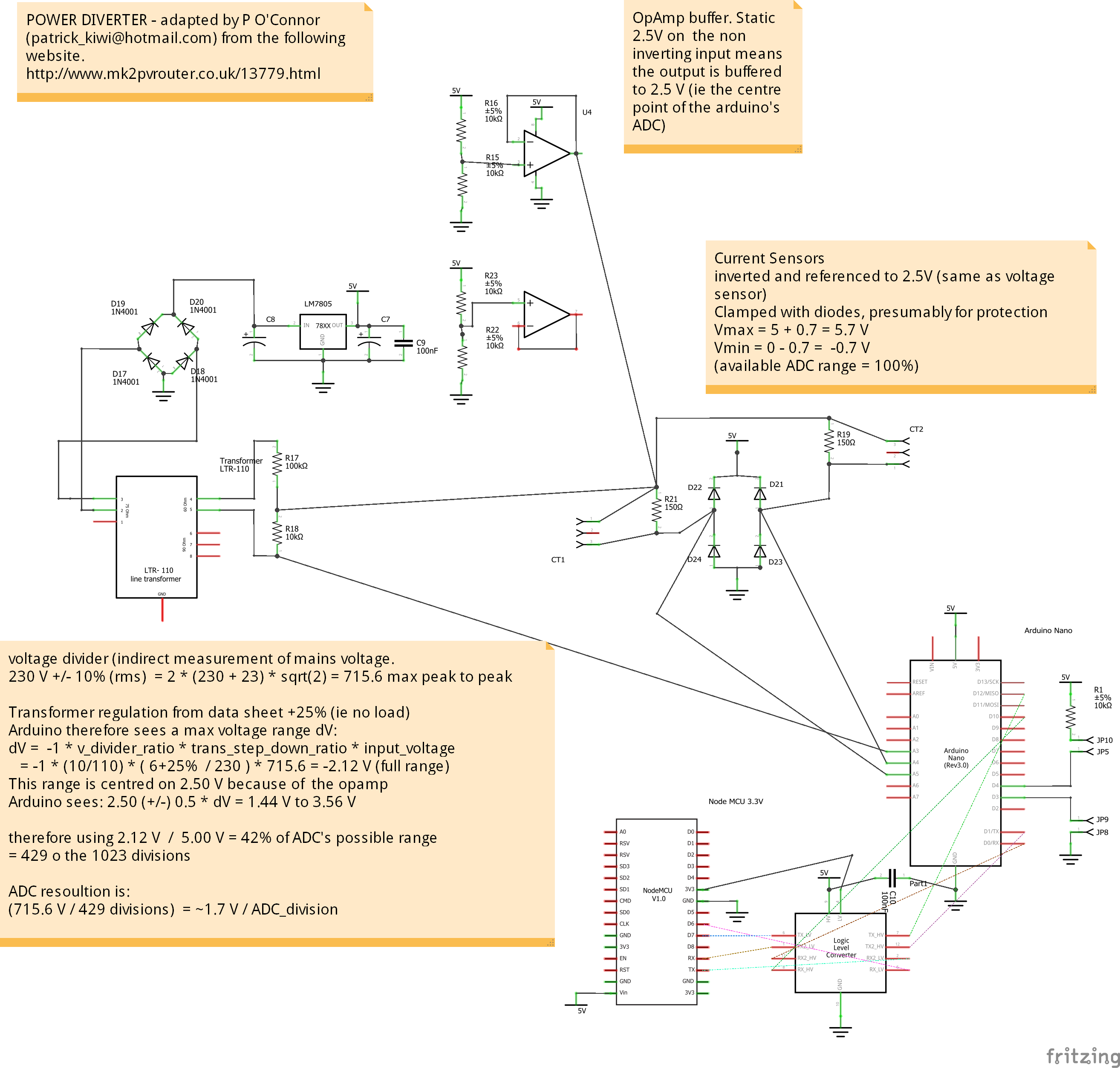
Here are my plans in Fritzing. I made some notes on the schematic (which was pretty much copied from Robin Emley’s design). Would be great if someone could check them out and comment. Could it be designed better? Are my notes correct? Why does the voltage sensor not have a diode clamp but the current sensors do? Why does the voltage sensor only use a small fraction of the Arduino’s ADC range?
Fritzing plans here:
Many thanks in advance
Patrick!
ps - thanks to Robert Wall for pointing out some mistakes in my schematic commentary - I’ve edited them because I don’t want to propagate incorrect information. I hope all is correct now!
I’ve elevated your privileges, so can you please load those diagrams here. There’s good reason for that - if at some point in the future they go away, everything else is pretty much meaningless and a lot of value that this thread would have had will be lost.
I didn’t design the input circuit, but it’s hardly likely that there will be a significant overvoltage on the voltage input, unless there’s a seriously bad source of interference present, or something like a lightning strike.
I think “a small fraction” is a bit of an exaggeration? I’ve not looked at the external website, but if you think that, I’d suspect an error in your calculations. Again, I didn’t design the input circuit, but it isn’t as if you’re desperate for resolution. Voltage can be expected to vary by ±10% from the nominal value at the most under normal conditions. It’s a different matter with the current, where a normal operating range is something like 1% to 80%, so you are desperate for resolution at the low end, and faced with a huge spike limited most likely by the c.t. saturating while the protective devices are clearing a downstream fault, at the high end.
We’ve never, to my knowledge, had a processor damaged due to excessive input current, but that’s not to say it’s impossible. If you wish to improve the protection on the inputs, feel free to do so. There’s been quite a lot of discussion in the past, I think you’ll find some of that here and some in the “Archived” section.
Thank you. That makes sense. I assumed that either my calculations were wrong, or it was designed in a super minimalist rugged way, and that more adc range simply wasn’t necessary.
Your clamping voltages are wrong - they clamp at -0.7 V and + 5.7 V (remember which way the voltages are when the diode is conducting). Those diodes might not offer full protection, because they’re not guaranteed to divert all the current away from the internal protection diodes. Check the forum threads for the full details. (Essentially, you need a highish value series resistor after your diodes to limit the current into the input to 1 mA, according to dBC, but not too high so as to avoid errors in the sample-and-hold process - see the Atmel data sheet.)
Your voltage calculations are also wrong:
Your starting point should be the maximum supply voltage, 230V + 10% (check this - ours in the UK is, or 240V +6% in olden times).
You’ve used the transformer ratio at full load - 6 / 230. The transformer will give you around 20 - 30% more than 6 V on no-load, it’s called “transformer regulation”. Check that with the supplier’s data sheet.
You also need to take component tolerances into account. There’s a ‘Learn’ page about that.
Check the supply voltages. Some ESP assemblies are 5 V tolerant, some aren’t, so you might not need the level converter.
That’s really helpful feedback. Thanks! I edited the schematic because I don’t want to propagate incorrect info. I guess from what you’re saying the clamping diodes may possibly be redundant without some series resistors, but I suppose they’re not doing any harm there. I noticed also that that the schematic from the EmonPi had a different protection circuit too. https://wiki.openenergymonitor.org/images/EmonP_V1.5_sch_white.png
What I’m really saying is they may well be ineffective without the series resistor. There’s already a protection diode inside the input (see the Atmel data sheet), but it is severely current-limited at 1 mA. According to the data sheet, the maximum voltage on a pin is 0.5 V outside the power rails - external silicon diodes will only start to clamp at about 0.65 V at 25°C, therefore you need that series resistor to ensure that the current (driven by a voltage of about 1 V - that’s the forward drop of a 1N4148 at 100 mA) is limited to about 1 mA, i.e. 1 kΩ minimum. The upper limit for the total series resistance including that one is 10 kΩ before errors become unacceptable.
I seem to remember that those aren’t ordinary silicon diodes in the emonTx & emonPi, they’re TVS devices.
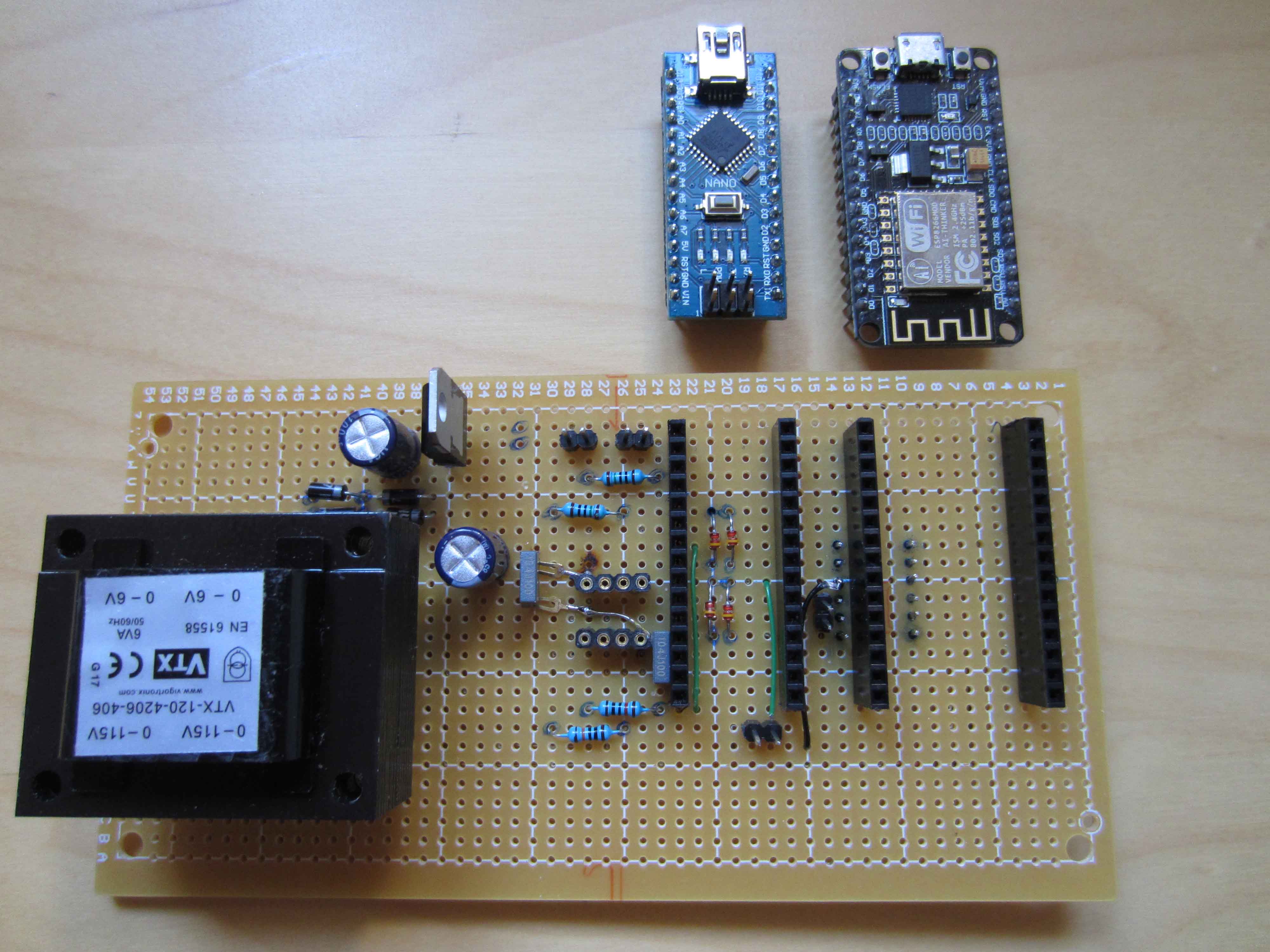
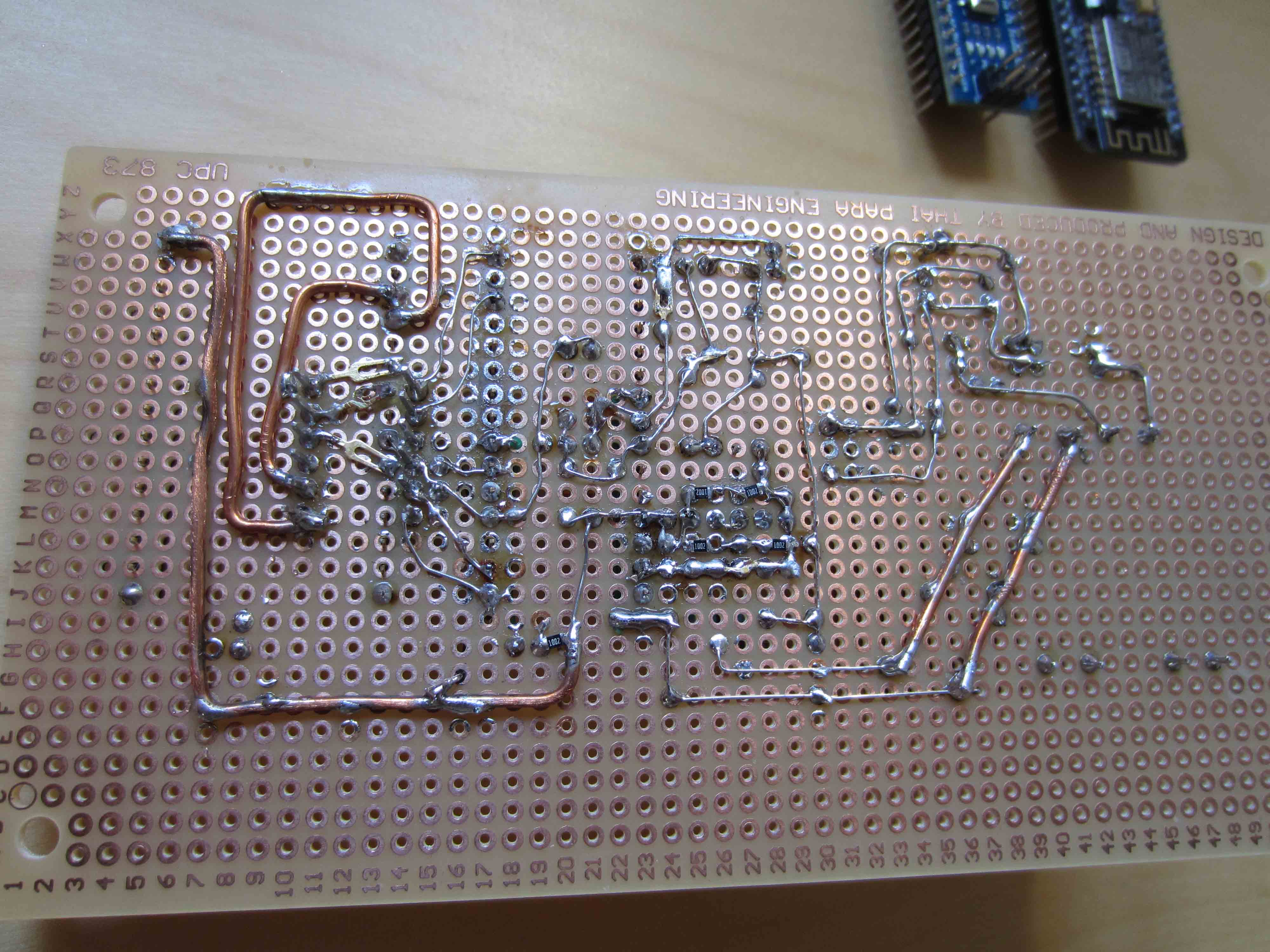
I think you should drill out the copper circles underneath the solid copper conductors - some of those look really close to each other - perhaps use some heat shrink or sleeve over the conductors?
Thanks, that’s a good idea. Yeah I know it’s a pretty bad construction. I didn’t have any wire so used the legs from the resistors, when they ran out I used some copper bits from a broken thing, and when they ran out I used some excessively thick copper wire I found half buried in some blackberry bushes at the local park. It’s not too bad though, photo doesn’t do it justice. if you look side on there’s about 0.5 - 1 mm of clearance everywhere.
hmm so in the event of a large current spike, even a short lived one, the current and forward voltage drop across the clamping diode may momentarily increase quite a bit, and therefore the diode may not offer much protection. Therefore to achieve protection you may need series resistors before and after the diodes perhaps as suggested in this forum Protecting ADC Input with Diode Clamp? - Page 1
but that may degrade the weak signal.
(24.6.1) Page 244 says: "The ADC is optimized for analog signals with an output impedance of approximately 10 kΩ or less. If such a source is used, the sampling time will be negligible. "
True, but they’re saying that the TOTAL source impedance should be less than 10 kΩ. That includes any series resistor, the external impedance is the impedance of the bias source (i.e. the capacitor, plus the signal source - 22 Ω in the case of the current input, and essentially 10 kΩ for the voltage input. When you read closely, it says it affects the least significant bit, and the mechanism is it limits the rate at which the S&H capacitor charges - too big and it won’t reach the input voltage before the multiplexer takes the input away. So I don’t see a problem with adding 1 kΩ in series with both current and voltage inputs. The voltage input is always about 75% of full scale - so no real problem there, where it just might be a concern is with very small currents, and to be honest, the bigger problem there is supply decoupling and noise. The emonTx V3.4 was looked at very carefully for that, yet we still see a few tens of mA (equivalent) of ‘noise current’.
 I hope all is correct now!