STM32 Development

I don’t have a problem there. This particular use has to be pretty thin on the ground, as compared to all the possible places I can think of where simultaneous is an absolute requirement. Like your 'scope - and that’s without trying.

What we’re looking at doing is using the capabilities of the processor to overcome shortcomings in the transducers. We can’t get away from those, and we can’t significantly reduce them even, without a significant cost penalty.

What I mean though is that if you can trigger the individual ADCs off the same Timer signal, and they’re running with the same clock, why do they need a special “Synchronised Mode”. It seems they’d be naturally synchronised with just the existing tricks. Although Sychronised Mode does let you fetch the two results at once in a single 32-bit read, so I guess that’s helpful for bus bandwidth etc. At these crazy high sampling speeds I can imagine all those internal busses are starting to get a bit busy.

I was guessing that “Synchronised” is better than simply started at the same instant. I’ve no idea though whether that’s valid.

ADC Tutorial Part2, fixing the Makefile and flashing an image

This post is likely platform dependent. @pb66 if you want to add any of your Windows findings, feel free to just edit it into this post if you think appropriate.

The “Makefile” selection in the Toolchain/IDE above is a new feature, and still a bit buggy at least on my Linux machine. Ideally, after Step 3 above, you’d be able just type ‘make’ in your project directory, and it would build your image e.g build/OEM.bin ready for flashing to your Nucleo.

If your link stage bombs out with lots of multiply defined symbols, open the Makefile in a text editor and check the list of files in the C_SOURCES variable. Remove all the duplicates.

If you get an error about the compiler not being found in the root directory, that’s because the BINPATH variable is not set. A solution I came across in the stm forums was to add this line to your Makefile, on the next line after the "all:’ line and before the “build the application” comment:

-include $(TARGET).mak

Then you can create a file in the project directory, right alongside the Makefile called project_name.mak and put your own directives/fixes in there. Here’s my OEM.mak:

BINPATH = /usr/bin
CFLAGS += -std=gnu99
LDFLAGS += -Xlinker --no-wchar-size-warning

WIth all that done, you should be able to type ‘make’ and get a clean build. To flash resultant binary onto your Nucleo board, simply copy it to the USB mass storage device like:

$ cp build/OEM.bin /media/dbc/NODE_F303RE/

One warning about the Makefile, it doesn’t seem to have built up the proper dependency rules based on which .c files include which .h files, so if you change a .h file you might want to do a

$ make clean
rm -fR .dep build
$ 

before issuing the make command. Note that ‘make clean’ completely nukes the build directory, so never put anything in there that you want to keep.

Coming up next… the /* USER CODE BEGIN */ additions to actually make the image do something, other than initialise HAL and hardware… finally!

1 Like

I thought that might be the case.

Thanks for the links Paul.

I will take another look at this tomorrow, am I the only one using windows? I know dBC isn’t, Trystan and Glyn will both be using Linux, perhaps I can find a better (non-windows) way of doing it.

3. ADC Tutorial Part3, adding user code to make it useful.

Once you’ve got a clean build out of part 2, it’s time to actually write your own code to make it do something useful. Actually, this ADC example doesn’t do anything useful, other than start the ADC running and monitor how often the data comes in, but it hopefully forms a good starting point for getting the ADC started and then adding your own code. You should always add your code only in the areas provided in the generated source, denoted by comments like /* USER CODE BEGIN n / / USER CODE END n */, thereby ensuring your code won’t get clobbered next time you need to regenerate via the GUI (double check you’ve ticked the relevant tick box in the Panel in Step 3 of Part 1 to ensure that).

I’ll attach a tar file of the Src and Inc directories at the end so you can have something concrete that compiles. But it goes roughly like this:

in main.c before the infinite loop starts (so a bit like Arduino’s setup()):

  /* USER CODE BEGIN 2 */

  HAL_GPIO_WritePin(LD2_GPIO_Port, LD2_Pin, GPIO_PIN_SET);      // LED on
  
  snprintf(log_buffer, sizeof(log_buffer),
	   "\nOEM ADC Demo 1.0\n");
  debug_printf(log_buffer);
  calibrate_ADC2();
  start_ADC2();

  /* USER CODE END 2 */

in main.c the infinite loop (so a bit like Arduino’s loop()):

  /* Infinite loop */
  /* USER CODE BEGIN WHILE */
  while (1)
  {
    if (adc2_half_conv_complete && !adc2_half_conv_overrun) {
      HAL_GPIO_WritePin(LD2_GPIO_Port, LD2_Pin, GPIO_PIN_RESET);      // LED off
      adc2_half_conv_complete = false;                                // ready for the next batch
    }

    if (adc2_full_conv_complete && !adc2_full_conv_overrun) {
      HAL_GPIO_WritePin(LD2_GPIO_Port, LD2_Pin, GPIO_PIN_SET);        // LED on
      adc2_full_conv_complete = false;
    }

    //
    // See if we've overrun and lost our place.
    //
    if (adc2_half_conv_overrun || adc2_full_conv_overrun) {
      snprintf(log_buffer, sizeof(log_buffer), "Data overrun!!!\n");
      debug_printf(log_buffer);
      adc2_full_conv_complete = adc2_half_conv_complete =
	adc2_full_conv_overrun = adc2_half_conv_overrun = false;
    }

  /* USER CODE END WHILE */

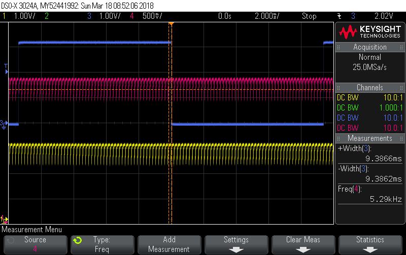
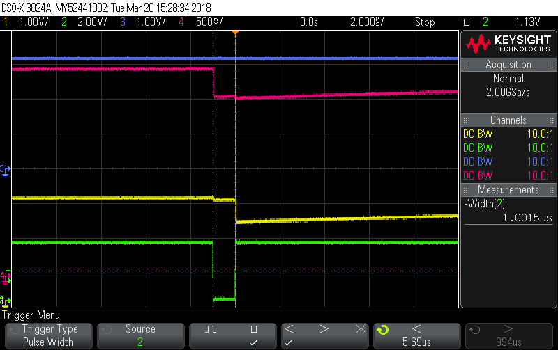
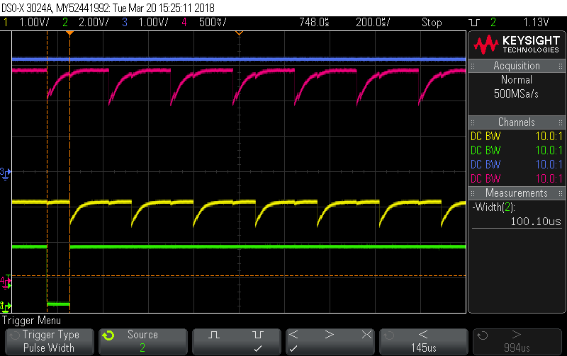
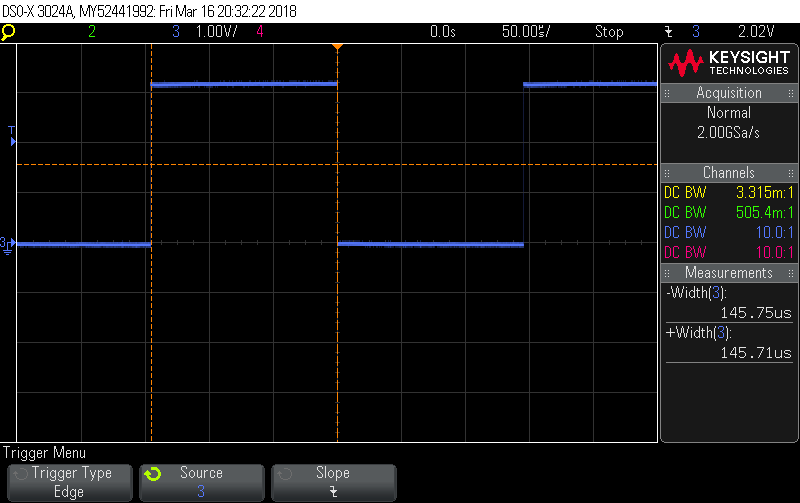
Those four adc2_xxx_conv_xxx boolean flags are all flags set in the DMA ISR (below). The half version tells us the bottom half of the array has just been filled with conversions, and the full version tells us the top half of the array has just been filled with conversions. They’re cleared here in the main loop to acknowledge we’ve “processed them”. In fact, the only processing we do is turn the LED off when a new batch of data has arrived in the bottom half and turn it back on for the top half. It’s all happening way too fast for you to see that with the naked eye, but a scope on the LED reveals:

So a new batch of 50x15 readings is arriving every 146 usecs as theory predicts (50x15 x 14 cycles/conversion / 72MHz).

The rest happens in adc.c:

/* USER CODE BEGIN 0 */

volatile uint16_t adc2_dma_buff[ADC2_DMA_BUFFSIZE];
volatile bool adc2_half_conv_complete, adc2_full_conv_complete;
volatile bool adc2_half_conv_overrun, adc2_full_conv_overrun;

/* USER CODE END 0 */

ADC2_DMA_BUFFSIZE is15x100 from adc.h (also user code, that’s not some HAL setting). The booleans need to be volatile because they’re set by the ISR. The DMA buffer needs to be volatile because it’s being continuously written to by the DMA controller.

Still in adc.c, we have the two functions we called from main.c before we entered the infinite loop:

/* USER CODE BEGIN 1 */

...

void calibrate_ADC2 (void) {

  HAL_ADCEx_Calibration_Start(&hadc2, ADC_SINGLE_ENDED);
}

void start_ADC2 (void) {

  HAL_ADC_Start_DMA(&hadc2, (uint32_t*)adc2_dma_buff, ADC2_DMA_BUFFSIZE);
}

/* USER CODE END 1 */

If you check the hardware reference manual for the device, you’ll see the ADCs have a pretty complicated self-calibration process. Fortunately, it’ll all been implemented in the HAL by stm, just don’t forget to call it or you get lousy results.

The start routine is what kicks it all off. From the moment you call that, there’ll be a new conversion written somewhere in adc2_dma_buff[] every 194 nsecs forever… well until you call Stop and this example never does. This call is where you associate your data buffer with that DMA channel and tell it how big it is. Recall we configured it as “Circular” in the GUI which means instead of running off the end, it starts back at the beginning.

There’s no way of knowing where in the buffer the DMA is currently writing, except that we know: it writes sequentially from adc2_dma_buff[0] to adc2_dma_buff[1499] 16-bits at a time and generates a half-full interrupt as it writes to adc2_dma_buff[749] and a full interrupt as it writes to adc2_dma_buff[1499] but it just keeps on trucking whether you process the data or not. 194nsecs after writing to adc2_dma_buff[1499] it’ll be writing the next conversion to adc2_dma_buff[0]… on and on forever with no CPU intervention… even if you disable the notification interrupts, it just keeps trucking.

You can make the DMA buffer as big or as small as you like. The bigger you make it, the less frequent the interrupt rate will be and the more data you’ll have to process when they do occur, which is good for amortising the cost of the ISR overhead. Make it small enough and you’ll be doing nothing but servicing interrupts, especially at the crazy fast speeds this example is running the DAC.
[EDIT] - but make it a multiple of the number of channels in the ADC sequence thereby ensuring any particular position in the array will always correspond to the same channel. In this example it’s defined in adc.h like this:

/* USER CODE BEGIN Private defines */

#define ADC2_DMA_BUFFSIZE 15*100    // 15 samples in a sequence, 100 sequences
extern volatile uint16_t adc2_dma_buff[ADC2_DMA_BUFFSIZE];
extern volatile bool adc2_half_conv_complete, adc2_full_conv_complete;
extern volatile bool adc2_half_conv_overrun, adc2_full_conv_overrun;
   
/* USER CODE END Private defines */

Finally in adc.c are the handlers for the half-full and full-full interrupts:

/* USER CODE BEGIN 1 */
void HAL_ADC_ConvHalfCpltCallback(ADC_HandleTypeDef* hadc)
{
  //
  // If the flag is already set, process level has been too slow
  // clearing it down.
  //
  if (adc2_half_conv_complete) {
    adc2_half_conv_overrun = true;
    adc2_half_conv_complete = false;
  } else
    adc2_half_conv_complete = true;
}

void HAL_ADC_ConvCpltCallback(ADC_HandleTypeDef* hadc)
{
  //
  // If the flag is already set, process level has been too slow
  // clearing it down.
  //
  if (adc2_full_conv_complete) {
    adc2_full_conv_overrun = true;
    adc2_full_conv_complete = false;
  } else
    adc2_full_conv_complete = true;
}

...

/* USER CODE END 1 */

Normally that’s where you’d want to do some preliminary processing of the data in adc2_dma_buff[]. This example just notes its arrival so that the main loop can flash the LED.

You might wonder how just declaring two functions gets them linked into the ISR. Their names are special. The HAL has already declared two functions of the same name (that do nothing), but declared them WEAK. If you don’t provide these functions, the linker will resolve it to the WEAK version. If you do, the WEAK version disappears to allow your version (no doubly defined symbol errors, because one is defined WEAK).

Note also there’s no ADC2 in the name, just ADC. These two functions get called for all ADCs and it’s up to you to determine which ADC just passed a boundary by looking at the handle that is passed in. This example doesn’t bother doing that because there is only one ADC enabled.

There are other ways to do ISRs within the HAL boundaries. Have a look in Src/stm32f3xx_it.c. That’s where the actual ISRs live, i.e. those routines are what the vectors point to. And they too include /* USER CODE BEGIN */ so you can put your code in there, or you can use the Callback approach that this example uses.

There are two common gripes users have about HAL:

  1. uses a lot of RAM (all those init structures are static)
  2. interrupt latency

In this example I measured the latency to be about 2usecs and that’ll get slightly worse when you have to demux the incoming handle when you have more than one ADC pumping. If that’s an issue, moving your critical ISR code to Src/stm32f3xx_it.c can help.

Finally, debug_printf() is very simple it lives in usart.c and looks like:

/* USER CODE BEGIN 1 */

void debug_printf (char* p) {
  HAL_UART_Transmit(&huart2, (uint8_t*)p, strlen(p), 1000);
}

/* USER CODE END 1 */

I broke it out like that because some of my projects have other output devices that I sometimes want to send the debug messages out over. That ‘1000’ isn’t the length of the buffer, but rather the maximum time this routine should wait (in msecs) to get the message out through the UART. It’s a simple block-until-done interface so be careful where you call it. uart2 is hardwired to the st-link programmer strip at the top of the Nucleo board, and those messages will get sent all the way to the host via /dev/ttyACM0 etc.

When you fire up this program, you should see:

OEM ADC Demo 1.0

in your minicom window.

Oh, and finally, all these HAL routines return a status. This example ignores that and assumes the best, but probably shouldn’t.

Tar file of Src and Inc directories attached:
ADC_demo.tar.gz (12.5 KB)

Thanks again @dBC for taking the time to write the tutorial, I think I have it working! :slight_smile: I had to change ADC2 to ADC1, bool to unit16_t with a #define true 1 & #define false 0 as I kept getting error: ‘false’ undeclared and I commented out HAL_ADCEx_Calibration_Start(&hadc1, ADC_SINGLE_ENDED); it may not be available on the f401re?..

I also set these:

hadc1.Init.ClockPrescaler = ADC_CLOCK_SYNC_PCLK_DIV8;
sConfig.SamplingTime = ADC_SAMPLETIME_480CYCLES;

The LED is flashing at a visible rate

I have uploaded my code here: https://github.com/TrystanLea/STM32Dev

TBH @pb66, the cards are stacked against us Windows users when it comes to serious development, that’s why I tend to do most of my code work within a Oracle Virtualbox container running Debian 64 bit Linux, which runs pretty well on my Windows 10 laptop, and gives me the full range of developers tools, and helps me follow tutorials which have been prepared in Linux.
By installing vboxadditions it gives you full graphic support, USB access, copy/paste to/from Windows, plus lots of other features (I have a very easy install command for this if anyone is interested - much easier than the guide!).

Paul

debian

2 Likes

I just added:

  sprintf(log_buffer,"%i\r\n",adc1_dma_buff[800]);
  debug_printf(log_buffer);
  sprintf(log_buffer,"%i\r\n",adc1_dma_buff[801]);
  debug_printf(log_buffer);
  sprintf(log_buffer,"%i\r\n",adc1_dma_buff[802]);
  debug_printf(log_buffer);
  sprintf(log_buffer,"%i\r\n",adc1_dma_buff[803]);
  debug_printf(log_buffer);

in the adc1_full_conv_complete section in the main loop and I have some sensible readings (made possible with the slowed down ADC)

2038
1
2041
1
2037
0
...

The voltage input is at mid rail and there is no CT plugged in, the socket pulls the input to ground with no CT plugged in hence the near zero values.

Excellent… driving the inputs and looking at the data is one part I skipped in my testing :wink: And yes, slowing that ADC clock way down is the way to go once you’re trying to make real measurements… better to tune later from a low setting, than puzzle why readings don’t make sense from a fast setting.

Yes, I was a bit slack documenting some of the more mundane stuff. In my main.h I’d added the following, but didn’t mention it in the tutorial:

/* USER CODE BEGIN Includes */

#include <stdbool.h>
#include <inttypes.h>

/* USER CODE END Includes */

I think you’re correct, there’s no mention of ADC self calibration in the reference manual for your processor (RM0368). When I copied some of my old F091 ADC code to kickstart this F303 demo, I noticed there was a second parameter to that function on the F303. I just had a look at your stm Arduino pointer above and they’ve ifdef’d that call based on CPU type to 3 variants… 1 argument, 2 arguments, and no call at all.

And if you want to avoid the walking-across-the-screen syndrome without the \r on the end of all your strings, minicom has a ‘U’ option to automatically add a CR:

1 Like

So I wasn’t going crazy after all…

This is from the RS page for the Nucleo-64 and more specifically the STM32F303RET6, looking closer it does say “F3 family” but that one item is the only thing that doesn’t apply to the F303

Fast 12-Bit ADCs (5 MSPS per channel with up to 18MSPS in interleaved mode)
16-Bit sigma-delta ADCs
Fast 144MHz motor control timers, timing resolution better 7ns

Here are some pictures of what’s going on under the bonnet for those that way inclined. I’ve made some slight changes to the OEM demo code above:

  1. divide the ADC clock by 2, so now running at 36MHz
  2. increase the sampling time to 601.5 cycles
  3. removed the replications of channel ‘1’ in the scan sequence
  4. moved the LED toggle into the actual ISR to reduce latency

So the sampling maths for this set up is:

One conversion takes 601.5 cycles to charge the S&H cap plus another 12.5 cycles to do the conversion, 614 cycles at 36 MHz is 17 usecs per conversion.

The sequence is now only 11 channels rather than 15, because I now treat Ch1 the same as all the other channels (i.e. just sample it once). So a sequence now takes 11 x 17 usecs which is 188 usecs. That sequence period also gives us our per-channel sampling frequency, namely 5330 Hz which is much closer to where you want to be for measuring mains power, compared with the crazy high sampling speeds in the tutorial.

I’ve left the buffer at 100 sequences so we still get an interrupt every 50 sequences, which is now at a much more leisurely 9.4 msecs. The buffer is now 100x11 long rather than 100x15 long. I’ve added a note to the Tutorial above to ensure the buffer is always a multiple of the scan sequence length, otherwise channels don’t turn up in the same array position each time through.

These three pictures are all of the same thing, just at different timebases.

Blue - LED output toggled in data-ready ISR
Red - ADC input pin corresponding to slot 1 in the sequence
Yellow - ADC input pin corresponding to slot 11 (last) in the sequence

I did my trick of putting a 1M pull-up on the two analog input pins, but they’re otherwise undriven. That way you can easily see when they get selected for sampling… the voltage drops like a brick.

In this one you can see the interrupts are coming in at a leisurely 9.4 msecs and that the sampling rate on a given channel is a respectable 5.3 kHz:

This next one zooms in to show that time between the sample-start of the last slot (Yellow) and the sample-start of the following first-slot (Red) is 17 usecs:

And finally, the third one zooms in even further again to show that the interrupt latency after the sample-start of the first slot (which corresponds to the end of sampling of the last slot) is just 520 nsecs, and a good chunk of that will be the call to
HAL_GPIO_TogglePin(LD2_GPIO_Port, LD2_Pin);


To achieve that I did away with the callback routines and toggled it right in the ISR which is found in Src/stm32f3xx_it.c:

/**
* @brief This function handles DMA2 channel1 global interrupt.
*/
void DMA2_Channel1_IRQHandler(void)
{
  /* USER CODE BEGIN DMA2_Channel1_IRQn 0 */

  HAL_GPIO_TogglePin(LD2_GPIO_Port, LD2_Pin);

  /* USER CODE END DMA2_Channel1_IRQn 0 */

@Robert.Wall
I guess the next step is to start up a second ADC and use the same techniques to determine how precisely we can offset their start times, and also ensure they then stay in lock step at that timeshift. Are you still thinking 0.1° is sufficient resolution? So somewhere around 4-6 usecs resolution, depending on line frequency. I’ve not been paying enough attention but what is the approximate phase shift correction (in degrees) you currently need for your collection of VTs and CTs? Always less than say 5° for the worst case combo? Does Voltage need to be advanced or retarded?

The ADC in this F303 just gets better and better, it has h/w offset removal. You can program up a 12-bit value you want subtracted from all readings on a channel. My 1M pull-up was reading in the mid 3100’s:

dma_buff[0]:3165                                                                                                                  
dma_buff[0]:3151                                                                                                                  
dma_buff[0]:3155                                                                                                                  
dma_buff[0]:3156                                                                                                                  
dma_buff[0]:3163                                                                                                                  
dma_buff[0]:3155  

Then I programmed up an offset of 3000:

dma_buff[0]:156                                                                                                                   
dma_buff[0]:159                                                                                                                   
dma_buff[0]:171                                                                                                                   
dma_buff[0]:158                                                                                                                   
dma_buff[0]:151     

You can program it on the fly … -ish. You need to STOP continuous conversions while you write in a new value, and then set them going again. Once enabled, the ADC result goes from being unsigned to signed so can go negative. Sounds perfect for h/w assistance with the removal of the mid-rail voltage. The CPU is going to have nothing to do at this rate.

4 Likes

Thanks @dBC, should have a F303 arriving tomorrow, so I can move over to continuing learning and development with that. Interesting to see ‘under the bonnet’! its great to see that detail

Cool.

Yep, and it was kinda’ necessary learning in order to experiment with @Robert.Wall’s excellent suggestion which I finally got around to trying out:

That turned out to be surprisingly easy to implement on the F303 (probably all the families with multiple ADCs I suspect). The approach I took is to set up one of the timers (TIM8) in one-pulse PWM mode which allows you to output a precisely timed pulse. I’ve configured mine to generate a pulse of anywhere from 1usec to 1msec.

You then internally route TIM8’s output to all the ADCs via TRGO2 and tell them to trigger on that signal. Set one to trigger on the negative edge of the pulse and other to trigger on the positive edge of the pulse and voila… you can precisely control the time shift between the ADCs starting. Having done so, they stay lock-step at that displacement because they’re all running off the same clock.

In the following scope pictures, Green is the pulse output, Red is an analog pin mapped to first channel in ADC2’s sequence, Yellow is the same for ADC3. There’s no requirement to run the pulse output to a pin as it all get routed internally, but it makes debugging a lot easier. The analog pins just have 1M pull-ups again to ensure their start-of-sample is clearly visible.


1 usec displacement


100 usec displacement


1 msec displacement.

You can see in that last one ADC2 has got almost 4 samples in before ADC3 starts.

The sampling maths for this one is:
1 conversion takes 614 cycles @ 36MHz is 17 usecs
16 conversions per sequence takes 272 usecs
That gives a per-channel sampling frequency of 3.68 kHz.
50 sequences per half buffer gives an interrupt arrival rate of 13.6 msecs per ADC

I figured this time I should actually feed it a signal and look at the results to see it was doing as intended. I wired the signal generator to both input pins (so they’re both sampling the exact same signal) and generated a 50Hz sinewave. Here’s what I found in the dma buffers at the various timeshift settings:


0 usecs shift.

Those two are so close together you can barely tell there are two plots there, but a look at the data says both ADCs are getting very similar results:

0_usecs_data


1 usec displacement


10 usec displacement


100 usec displacement


1 msec displacement

So we can do phase-shifts on the fly entirely in the analog domain down to 1usec resolution (~0.02 degrees at 50Hz). Actually, you could go lower but that seemed a bit over the top. And it’s programmable on the fly… -ish. You need to stop the ADCs, reconfig the timer, and then restart the ADCs, so it’s not something you want to be doing a lot of if you’re into continuous sampling, but certainly it could be a runtime configuration parameter, it’s not as if it needs to be baked into the image.

Credit to Robert for the suggestion, and credit to STM32MXCube for the code. I mostly hit “Generate Source”.

3 Likes

So it looks as if a chunk of processing and the amplitude errors associated with interpolation will disappear. :+1:

And if that delay was stretched to about 90°; then, given a resistive load, it could accurately measure its own phase error and self-calibrate. (The big problem there is knowing you truly have a resistive load.)

Going back some way to your (@dBC ) question about phase errors, here are some collated figures for a.c. adapters, the later (black cable, moulded plug) SCT-013-000 and the SCT006 c.t’s. All show a phase lead.

You might like to think about the capacitive “transformer” (borrowing the term from the high voltage - 66kV upwards - fraternity) that should have, if the op.amp. circuit is designed correctly, a very small phase shift that’s independent of voltage (Old forum: https://openenergymonitor.org/forum-archive/node/1568.html.), but as it needs to be “home made”, there’s a big problem with input scale calibration.

%20Adapters%20Phase


I’ve previously noted the large variations over time in both the v.t’s and c.t’s; the real problem where the a.c. adapters are concerned is we’re specifying a part that is designed as a general purpose power supply, not a measuring instrument.

Yep, it’s almost like having your own programmable precision delay line on the signal.

Nice.

That and having a stable known line frequency. Unfortunately, the delay is measured in usecs rather than degrees.

Thanks for the refresher on the various sensor phase error performance.

While playing around with this phase-shift idea (via precisely timed ADC triggers) I came to the conclusion I needed a bit of “power maths” in order to see it in action. So I knocked up some basic Vrms, Irms, Papp, Preal, PF calculations and used the offset-removal techniques described in @Robert.Wall’s excellent paper here: emonLib Maths(extended).pdf.

I tried to make it emonTxShield friendly because I figured that would be a common starting point for everyone, so it supports 4 current inputs and 1 voltage input. I scheduled the ADC conversions as follows:

adc_schedule

Which means in the first slot in the sequence it does 3 CT conversions and a VT conversion. In the second slot it does the 4th CT, with a new VT conversion. I had to give ADC1 and ADC3 something to do during those slots, so I selected a couple of internal channels: Temperature and Vref although I’ve not even looked at the data that comes back in those slots.

At this stage there’s just single phase difference setting between V and all the I’s. In other words, I trigger ADC4 on the rising edge and the other three on the falling edge. Having different phase settings on different CT channels may prove challenging.

One slight hiccup is I need to get the V input onto an ADC of its own (ADC4) so I moved it across to PB14 like so:


The four CT inputs line up perfectly with the emonTxShield usage and to get V to work you just need to run a jumper wire from CN7.28 (PA0) to CN10.28(PB14):

The fact that V is also connected to PA0 doesn’t matter, as in this example it’s configured as an unused analog input, so doesn’t get in the way. So a single wire with a female jumper connector on each end should get you going with the shield.

The early results look promising, this is specifying a 3333 usec delay between ADC4 and all the others like this:

  start_ADCs(3333);                 // start ADC with x usec lag

That should give ~60° phase shift. And with my signal generator sinewave feeding all 5 inputs the results look good:

0: Vrms: 1234.22, Irms: 1234.44, Papp: 1523560.12, Preal: 761240.69, PF: 0.500                               
1: Vrms: 1234.22, Irms: 1234.06, Papp: 1523093.12, Preal: 761020.94, PF: 0.500                               
2: Vrms: 1234.22, Irms: 1234.21, Papp: 1523286.88, Preal: 761084.25, PF: 0.500                               
3: Vrms: 1234.22, Irms: 1234.03, Papp: 1523063.00, Preal: 760992.19, PF: 0.500   

All numbers are in raw ADC units.

I’ll attach the Src/Inc/build directories here after a bit of a clean up, feel free to use as much or as little of them as you like. I was not sure whether the quietness on this thread was a good sign (everyone’s madly coding) or a bad sign (everyone’s stuck in the mysteries of HAL calls). If the former, feel free to ignore this code, if the latter, it’ll hopefully get you unstuck. If you just want to play with your own power calculation libraries, it should be hopefully easy enough to hook it in instead of my cheap-n-cheery power calculations.
txshield_demo.tar.gz (240.3 KB)

2 Likes

Sorry for disappearing, I’ve been to hell and back trying to get the toolchain sorted, with numerous obstacles coming between me and what I had hoped to be a straight forward and well documented task, well I guess it is was “well documented” there are literally thousands of guides and possibly no 2 are the same. But I’m there now.

I think there might be a minor omission in the tutorial above as I was getting some errors about log_buffer undeclared, I see in both your (@dBC) ADC_demo.tar.gz and @Trystan’s repo there is

/* Private variables ---------------------------------------------------------*/

char log_buffer[100];

/* USER CODE BEGIN PV */

but I missed that in the tutorial, I won’t stick my neck out and say it’s not there, but I have failed to find it despite looking many times.

So I’ve caught up to the end of 3. ADC Tutorial Part3, adding user code to make it useful. and I have added both the “log_buffer fix” above and the “bools fix” 4 posts on from the end of Part3 .

but from there I’m unsure if you and Trystan are collaborating on shared code or doing separate things, I’m sure with some trial and error I might work it out (although I’ve had enough trial and error this week to last a lifetime) but it would be useful to know if this is still one example or not.